Microchip ATmega3208 AVR MCU开发方案
 112
112
 拍明
拍明
原标题:Microchip ATmega3208 AVR MCU开发方案
microchip公司的ATmega3208/3209微处理器是采用AVR®处理器的megaAVR® 0系列中一员,具有硬件乘法器,工作频率高达20MHz,提供各种闪存(高达48KB),SRAM(高达6KB)和256B EEPROM,以及采用28引脚,32引脚,40引脚或48引脚封装.闪存读写周期10000次,EEPROM 100,000次, 55℃时数据保存期为40年.可配置定制逻辑(CCL)有多达四个可编查找边(LUT).器件还集成了带可选择基准输入的模拟比较器(AC),10比特150ksps ADC,5个可选择内部电压基准: 0.55V, 1.1V, 1.5V, 2.5V和4.3V,多达41个可编程I/O线,具有汽车应用的AEC-Q100规范.工作温度-40℃ 到 +125℃:本文介绍了ATmega3208主要特性,框图以及开发板AVR-BLE主要特性,电路图和PCB装配图.
The ATmega3208/3209 microcontrollers are part of the megaAVR® 0-series, which uses the AVR® processor with hardware multiplier running at up to 20 MHz, and offers a wide range of Flash sizes up to 48 KB, up to 6 KB of SRAM, and 256 bytes of EEPROM in 28-, 32-, 40-, or 48-pin packages. The series uses the latest technologies from Microchip with a flexible and low-power architecture, including Event System and SleepWalking, accurate analog features, and advanced peripherals.
The devices described in this data sheet offer 32 KB in a 28/32/48-pin package.
ATmega3208主要特性:
• AVR® CPU:
– Single-cycle I/O access
– Two-level interrupt controller
– Two-cycle hardware multiplier
• Memories:
– 32 KB In-system self-programmable Flash memory
– 256B EEPROM
– 6 KB SRAM
– Write/Erase endurance:
• Flash 10,000 cycles
• EEPROM 100,000 cycles
– Data retention: 40 years at 55°C
• System:
– Power-on Reset (POR) circuit
– Brown-out Detector (BOD)
– Clock options:
• 16/20 MHz low-power internal oscillator
• 32.768 kHz Ultra Low-Power (ULP) internal oscillator
• 32.768 kHz external crystal oscillator
• External clock input
– Single-pin Unified Program Debug Interface (UPDI)
– Three sleep modes:
• Idle with all peripherals running for immediate wake-up
• Standby
– Configurable operation of selected peripherals
– SleepWalking peripherals
• Power-Down with limited wake-up functionality
• Peripherals:
– One 16-bit Timer/Counter type A (TCA) with a dedicated period register and three compare channels
– Up to four 16-bit Timer/Counters type B (TCB) with input capture
– One 16-bit Real-Time Counter (RTC) running from an external crystal or an internal RC oscillator
– Up to four USARTs with fractional baud rate generator, auto-baud, and start-of-frame detection
– Master/slave Serial Peripheral Interface (SPI)
– Master/slave TWI with dual address match
• Can operate simultaneously as master and slave
• Standard mode (Sm, 100 kHz)
• Fast mode (Fm, 400 kHz)
• Fast mode plus (Fm+, 1 MHz)
– Event System for core independent and predictable inter-peripheral signaling
– Configurable Custom Logic (CCL) with up to four programmable Look-up Tables (LUT)
– One Analog Comparator (AC) with a scalable reference input
– One 10-bit 150 ksps Analog-to-Digital Converter (ADC)
– Five selectable internal voltage references: 0.55V, 1.1V, 1.5V, 2.5V, and 4.3V
– CRC code memory scan hardware
• Optional automatic CRC scan before code execution is allowed
– Watchdog Timer (WDT) with Window mode, with a separate on-chip oscillator
– External interrupt on all general purpose pins
• I/O and Packages:
– Up to 41 programmable I/O lines
– 28-pin SSOP
– 32-pin VQFN 5x5 and TQFP 7x7
– 48-pin UQFN 6x6 and TQFP 7x7
• Temperature Ranges:
– Industrial: -40℃ to +85℃
– Extended: -40℃ to +125℃
• Speed Grades -40℃ to +105℃:
– 0-5 MHz @ 1.8V – 5.5V
– 0-10 MHz @ 2.7V – 5.5V
– 0-20 MHz @ 4.5V – 5.5V
• Speed Grades -40℃ to +125℃:
– 0-8 MHz @ 2.7V - 5.5V
– 0-16 MHz @ 4.5V - 5.5V
• VAO variants available: Designed, manufactured, tested, and qualified in accordance with AEC-Q100 requirements for automotive applications.
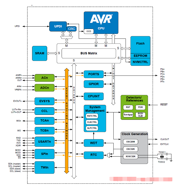
图1. ATmega3208框图
开发板AVR-BLE
The AVR-BLE Development Board is a small and easily expandable demonstration and development platform for Bluetooth® Low Energy (BLE) solutions based on the AVR® microcontroller architecture. It is designed to demonstrate that the design of a typical BLE application can be simplified by partitioning the task into three blocks:
• Smart – represented by the ATmega3208 microcontroller
• Secure – represented by the ATECC608A secure element
• Connected – represented by the RN4870 BLE module
In addition, the AVR-BLE Development Board features the following elements:
• The on-board debugger (PKoB nano) supplies full programming and debugging support through Atmel Studio/Microchip MPLAB® X IDE. It also provides access to a serial port interface (serial to USB bridge) and two logic analyzer channels (debug GPIO).
• A mikroBUS™ socket enables the ability to expand the board capabilities with the selection from 450+ sensors
and actuators options offered by MikroElektronika (www.mikroe.com) via a growing portfolio of Click board™.
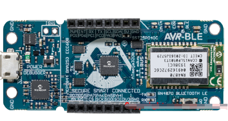
图2. 开发板AVR-BLE外形图
开发板AVR-BLE主要特性:
• ATmega3208 AVR Microcontroller
• Two User LEDs (Data and Error)
• Mechanical Button
• RN4870 Bluetooth Low Energy (BLE) Module
• MCP9844 Temperature Sensor
• BMA253 Acceleration Sensor
• ATECC608A CryptoAuthentication™ Device
• SST25PF040CT 4Mb Serial Flash
• mikroBUS Socket
• On-board Debugger
– Board identification in Atmel Studio/Microchip MPLAB® X IDE
– Programming and debugging
– Virtual serial port (USB CDC)
– Two logic analyzer channels (DGI GPIO)
• USB or Battery Powered
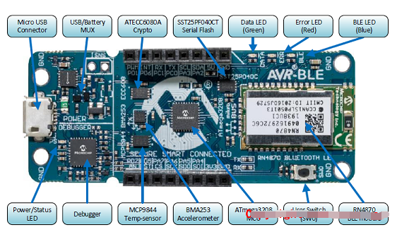
图3. 开发板AVR-BLE外形图(正面)
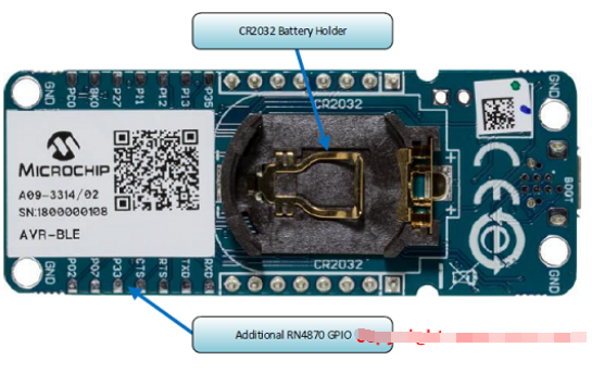
图4. 开发板AVR-BLE外形图(背面)
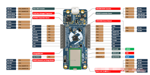
图5. 开发板AVR-BLE外形图(DT100111)
责任编辑:David
【免责声明】
1、本文内容、数据、图表等来源于网络引用或其他公开资料,版权归属原作者、原发表出处。若版权所有方对本文的引用持有异议,请联系拍明芯城(marketing@iczoom.com),本方将及时处理。
2、本文的引用仅供读者交流学习使用,不涉及商业目的。
3、本文内容仅代表作者观点,拍明芯城不对内容的准确性、可靠性或完整性提供明示或暗示的保证。读者阅读本文后做出的决定或行为,是基于自主意愿和独立判断做出的,请读者明确相关结果。
4、如需转载本方拥有版权的文章,请联系拍明芯城(marketing@iczoom.com)注明“转载原因”。未经允许私自转载拍明芯城将保留追究其法律责任的权利。
拍明芯城拥有对此声明的最终解释权。


 产品分类
产品分类




 2012- 2022 拍明芯城ICZOOM.com 版权所有 客服热线:400-693-8369 (9:00-18:00)


