


 产品分类
产品分类
ADI HSC-ADC-EVALC高速转换器评估方案
 88
88
 拍明
拍明
原标题:ADI HSC-ADC-EVALC高速转换器评估方案
ADI公司的HSC-ADC-EVALC高速转换器评估平台是基于Xilinx公司的Virtex-4 FPGA (XC4VFX20-10FFG672C)器件,该FPGA能通过VisualAnalog进行编程,以及能和各种高速数模转换器(ADC)配合.另一个主要器件是Cypress公司的USB器件,它能和主PC进行通信,并提供SPI接口进行配置.该平台支持1.8 V, 2.5 V和3.3 V CMOS以及LVDS接口,并行输入644MSPS SDR和800MSPS DDR,支持多达18位的多路ADC,进行实时的FFT和时域分析,以及分析SNR,SINAD,SFDR和失真等性能.本文介绍了HSC-ADC-EVALC高速转换器评估平台的主要特性,产品亮点以及方框图,系统应用案例和评估平台的详细电路图.
The HSC-ADC-EVALC evaluation platform is based around the Virtex-4 FPGA (XC4VFX20-10FFG672C) from Xilinx, which can be programmed through VisualAnalog to operate with a variety of data converters. Another key component, the Cypress USB device (U3), communicates with a host PC and provides the SPI interface used for configuration.
The HSC-ADC-EVALCZ high speed converter evaluation platform uses an FPGA based buffer memory board to capture blocks of digital data from the Analog Devices high speed analog-to-digital converter (ADC) evaluation boards. The board is connected to the PC through a USB port and is used with VisualAnalog to quickly evaluate the performance of high speed ADCs. The evaluation kit is easy to set up. Additional equipment needed includes an Analog Devices high speed ADC evaluation board, a signal source, and a clock source. Once the kit is connected and powered, the evaluation is enabled instantly on the PC.
HSC-ADC-EVALC主要特性:
Xilinx Virtex-4 FPGA-based buffer memory board
Used for capturing digital data from high speed ADC evaluation boards to simplify evaluation
64 kB FIFO depth
Parallel input at 644 MSPS SDR and 800 MSPS DDR
Supports 1.8 V, 2.5 V, and 3.3 V CMOS and LVDS interfaces
Supports multiple ADC channels up to 18 bits
Measures performance with VisualAnalog
Real-time FFT and time domain analysis
Analyzes SNR, SINAD, SFDR, and harmonics
Simple USB port interface (2.0)
Supports ADCs with serial port interfaces (SPI)
FPGA reconfigurable via JTAG, on-board EPROM, or USB
On-board regulator circuit speeds setup
5 V, 3 A switching power supply included
Compatible with Windows 98 (2nd edition), Windows 2000, Windows ME, and Windows XP
EQUIPMENT NEEDED
Analog signal source and antialiasing filter
Low jitter clock source
High speed ADC evaluation board and ADC data sheet
PC running Windows 98 (2nd edition), Windows 2000, Windows ME, or Windows XP
Latest version of VisualAnalog
USB 2.0 port recommended (USB 1.1 compatible)
HSC-ADC-EVALC亮点:
1. Easy to Set Up. Connect the included power supply along with the CLK and AIN signal sources to the two evaluation boards. Then connect to the PC via the USB port and evaluate the performance instantly.
2. USB Port Connection to PC. PC interface is via a USB 2.0 connection (1.1 compatible) to the PC. A USB cable is provided in the kit.
3. 64 kB FIFO. The on-board FPGA contains an integrated FIFO to store data captured from the ADC for subsequent processing.
4. Up to 644 MSPS SDR/800 MSPS DDR Encode Rates on Each Channel. Multichannel ADCs with encode rates up to 644 MSPS SDR and 800 MSPS DDR can be used with the ADC capture board.
5. Supports ADCs with Serial Port Interface or SPI. Some ADCs include a feature set that can be changed via the SPI. The ADC capture board supports these SPI-driven features through the existing USB connection to the computer without additional cabling needed.
6. VisualAnalog. VisualAnalog supports the HSC-ADC-EVALC hardware platform as well as enabling virtual ADC evaluation using ADIsimADC™, Analog Devices proprietary behavioral modeling technology. This allows rapid compari-son between multiple ADCs, with or without hardware evaluation boards.

图1.HSC-ADC-EVALC功能方框图

图2.HSC-ADC-EVALC ADC捕捉板和ADC评估板应用案例

图3.HSC-ADC-EVALC外形图
HSC-ADC-EVALC SCHEMATICS
005TYCO AND DSP EZ–KIT CONNECTOR TO FPGAXC4VFX20-

图4.HSC-ADC-EVALC电路图(1)

图5.HSC-ADC-EVALC电路图(2)

图6.HSC-ADC-EVALC电路图(3)

图7.HSC-ADC-EVALC电路图(4)

图8.HSC-ADC-EVALC电路图(5)
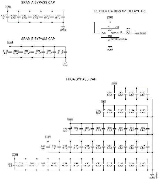
图9.HSC-ADC-EVALC电路图(6)

图10.HSC-ADC-EVALC电路图(7)

图11.HSC-ADC-EVALC电路图(8)

图12.HSC-ADC-EVALC电路图(9)

图13.HSC-ADC-EVALC电路图(10)

图14.HSC-ADC-EVALC电路图(11)

图15.HSC-ADC-EVALC电路图(12)

图16.HSC-ADC-EVALC电路图(13)

图17.HSC-ADC-EVALC电路图(14)
责任编辑:David
【免责声明】
1、本文内容、数据、图表等来源于网络引用或其他公开资料,版权归属原作者、原发表出处。若版权所有方对本文的引用持有异议,请联系拍明芯城(marketing@iczoom.com),本方将及时处理。
2、本文的引用仅供读者交流学习使用,不涉及商业目的。
3、本文内容仅代表作者观点,拍明芯城不对内容的准确性、可靠性或完整性提供明示或暗示的保证。读者阅读本文后做出的决定或行为,是基于自主意愿和独立判断做出的,请读者明确相关结果。
4、如需转载本方拥有版权的文章,请联系拍明芯城(marketing@iczoom.com)注明“转载原因”。未经允许私自转载拍明芯城将保留追究其法律责任的权利。
拍明芯城拥有对此声明的最终解释权。
相关资讯
:
基于MC33771主控芯片的新能源锂电池管理系统解决方案

AMIC110 32位Sitara ARM MCU开发方案

基于AMIC110多协议可编程工业通信处理器的32位Sitara ARM MCU开发方案

基于展讯SC9820超低成本LTE芯片平台的儿童智能手表解决方案

基于TI公司的AM437x双照相机参考设计

基于MTK6580芯片的W2智能手表解决方案


 2012- 2022 拍明芯城ICZOOM.com 版权所有 客服热线:400-693-8369 (9:00-18:00)


