


 产品分类
产品分类
Renesas RX23W32位RX MCU应用方案
 159
159
 拍明
拍明
原标题:Renesas RX23W32位RX MCU应用方案
Renesas公司的RX23W是54MHz 32位RX mcu,内置了FPU(和IEEE75兼容),54 MHz时的性能为88.56 DMIPS;集成了高达512KB闪存,Bluetooth 5.0以及多种通信功能如USB 2.0全速主/功能/OTG,CAN,SD主接口,串行声接口,容性触摸检测单元,12位ADC,12位DAC以及RTC和加密功能.RX23W的CISC哈佛架构具有5级流水线,可变长度指令和超紧凑代码,片上集成了调试电路,支持存储器保护单元(MPU)和温度传感器.单电源1.8-V-3.6-V工作,工作温度-40到+85度C.有三种降功耗模式.主要用在通用工业和消费类电子设备.本文介绍了RX23W主要特性和特性指标表,框图以及RX23W目标板RTK5RX23W0C00000BJ主要特性和指标,框图与运行环境图,电路图和材料清单与元件布局图.
RX23W microcontrollers incorporate security functions that are vital for Bluetooth® 5.0 Low Energy (BLE) and IoT devices, as well as a wealth of peripheral functions such as touch keys, USB and CAN, enabling system control and wireless communication with devices using a single chip. RX23W MCUs have full function support for Bluetooth 5.0 Low Energy long range and mesh networking, and provide excellent reception performance.
RX23W主要特性:
■ 32-bit RXv2 CPU core
Max.operating frequency: 54 MHz
Capable of 88.56 DMIPS in operation at 54 MHz
Enhanced DSP: 32-bit multiply-accumulate and 16-bitmultiply-subtract instructions supported
Built-in FPU: 32-bit single-precision floating point (compliant toIEEE754)
Divider (fastest instruction execution takes two CPU clock cycles)
Fast interrupt
CISC Harvard architecture with 5-stage pipeline
Variable-length instructions, ultra-compact code
On-chip debugging circuit
Memory protection unit (MPU) supported
■ Low power design and architecture
Operation from a single 1.8-V to 3.6-V supply
RTC capable of operating on the battery backup power supply
Three low power consumption modes
Low power timer (LPT) that operates during the software standby state
■ On-chip flash memory for code
384- to 512-Kbyte capacities
On-board or off-board user programming
Programmable at 1.8 V
For instructions and operands
■ On-chip data flash memory
8 Kbytes (1,000,000 program/erase cycles (typ.))
BGO (Background Operation)
■ On-chip SRAM, no wait states
64-Kbyte size capacities
■ Data transfer functions
DMAC: Incorporates four channels
DTC: Four transfer modes
■ ELC
Module operation can be initiated by event signals without usinginterrupts.
Linked operation between modules is possible while the CPU is sleeping.
■ Reset and supply management
Eight types of reset, including the power-on reset (POR)
Low voltage detection (LVD) with voltage settings
■ Clock functions
Main clock oscillator frequency: 1 to 20 MHz
External clock input frequency: Up to 20 MHz
Sub-clock oscillator frequency: 32.768 kHz
Frequency of Bluetooth-dedicated clock oscillator: 32 MHz
PLL circuit input: 4 MHz to 12.5 MHz
On-chip low- and high-speed oscillators, dedicated on-chip low-speedoscillator for the IWDT
USB-dedicated PLL circuit: 4, 6, 8, or 12 MHz
54 MHz can be set for the system clock and 48 MHz for the USB clock
Generation of a dedicated 32.768-kHz clock for the RTC
Clock frequency accuracy measurement circuit (CAC)
■ Realtime clock
Adjustment functions (30 seconds, leap year, and error)
Calendar count mode or binary count mode selectable
Time capture function
Time capture on event-signal input through external pins
■ Independent watchdog timer
15-kHz on-chip oscillator produces a dedicated clock signal to driveIWDT operation.
■ Useful functions for IEC60730 compliance
Self-diagnostic and disconnection-detection assistance functions forthe A/D converter, clock frequency accuracy measurement circuit,independent watchdog timer, RAM test assistance functions using theDOC, etc.
■ MPC
Input/output functions selectable from multiple pins
■ Up to 12 communication functions
Bluetooth Low Energy (1 channel)
An RF transceiver and link layer compliant with the Bluetooth 5.0 LowEnergy specification
LE 1M PHY, LE 2M PHY, LE Coded PHY (125 kbps and 500 kbps),and LE Advertising extension support
On-chip Bluetooth-dedicated AES-CCM (128-bit blocks) encryptioncircuit
USB 2.0 host/function/On-The-Go (OTG) (one channel),full-speed = 12 Mbps, low-speed = 1.5 Mbps, isochronous transfer, andBC (Battery Charger) supported
CAN (one channel) compliant to ISO11898-1:Transfer at up to 1 Mbps
SCI with many useful functions (up to 4 channels)
Asynchronous mode, clock synchronous mode, smart card interface
Reduction of errors in communications using the bit modulationfunction
IrDA interface (one channel, in cooperation with the SCI5)
I2C bus interface: Transfer at up to 400 kbps, capable of SMBusoperation (one channel)
RSPI (one channel): Transfer at up to 16 Mbps
Serial sound interface (one channel)
SD host interface (optional: one channel) SD memory/ SDIO 1-bit or4-bit SD bus supported
■ Up to 19 extended-function timers
16-bit MTU: input capture, output compare, complementary PWMoutput, phase counting mode (five channels)
16-bit TPU: input capture, output compare, phase counting mode (sixchannels)
8-bit TMR (four channels)
16-bit compare-match timers (four channels)
■ 12-bit A/D converter
Capable of conversion within 0.83 μs
14 channels
Sampling time can be set for each channel
Self-diagnostic function and analog input disconnection detectionassistance function
■ 12-bit D/A converter
Two channels
■ Capacitive touch sensing unit
Self-capacitance method: A single pin configures a single key,supporting up to 12 keys
Mutual capacitance method: Matrix configuration with 12 pins, supportingup to 36 keys
■ Analog comparator
Two channels × one unit
■ General I/O ports
5-V tolerant, open drain, input pull-up, switching of driving capacity
■ Encryption functions (TSIP-Lite)
Unauthorized access to the encryption engine is disabled andimposture and falsification of information are prevented
Safe management of keys
128- or 256-bit key length of AES for ECB, CBC, GCM, others
True random number generator
■ Temperature sensor
■ Operating temperature range
40 to +85C
RX23W应用:
General industrial and consumer equipment
RX23W主要指标特性表:
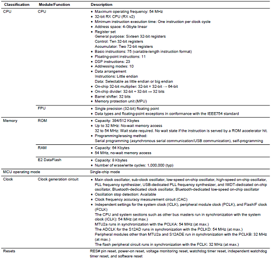


图1.RX23W框图
RX23W目标板RTK5RX23W0C00000BJ
Thank you for purchasing the Target Board for RX23W evaluation tool from Renesas (hereinafter referred to as “this product”). This product consists of the Target Board for RX23W (RTK5RX23W0C00000BJ).
This product is an evaluation tool for a Renesas MCU. This manual descries hardware specifications, how to set switches, and basic setup procedures.
RX23W目标板主要特性:
• Programming of the Renesas MCU
• Debugging of user code
• Evaluation of Bluetooth Low Energy (BLE) communications
• User circuits for switches and LEDs
• Sample applications*1
• Samples of peripheral-function initialization code*
RX23W目标板主要指标:


图2. RX23W目标板框图

图3.RX23W目标板顶层布局图

图4.RX23W目标板运行环境图
RX23W目标板材料清单:

责任编辑:David
【免责声明】
1、本文内容、数据、图表等来源于网络引用或其他公开资料,版权归属原作者、原发表出处。若版权所有方对本文的引用持有异议,请联系拍明芯城(marketing@iczoom.com),本方将及时处理。
2、本文的引用仅供读者交流学习使用,不涉及商业目的。
3、本文内容仅代表作者观点,拍明芯城不对内容的准确性、可靠性或完整性提供明示或暗示的保证。读者阅读本文后做出的决定或行为,是基于自主意愿和独立判断做出的,请读者明确相关结果。
4、如需转载本方拥有版权的文章,请联系拍明芯城(marketing@iczoom.com)注明“转载原因”。未经允许私自转载拍明芯城将保留追究其法律责任的权利。
拍明芯城拥有对此声明的最终解释权。
相关资讯
:
基于MC33771主控芯片的新能源锂电池管理系统解决方案

AMIC110 32位Sitara ARM MCU开发方案

基于AMIC110多协议可编程工业通信处理器的32位Sitara ARM MCU开发方案

基于展讯SC9820超低成本LTE芯片平台的儿童智能手表解决方案

基于TI公司的AM437x双照相机参考设计

基于MTK6580芯片的W2智能手表解决方案


 2012- 2022 拍明芯城ICZOOM.com 版权所有 客服热线:400-693-8369 (9:00-18:00)


