ST ST25DV04 NFC RFID标签解决方案
 137
137
 拍明
拍明
原标题:ST ST25DV04 NFC RFID标签解决方案
ST公司的st25DV04K,ST25DV16K和ST25DV64K(ST25DVxxx)是NFC RFID标签,代表4Kb,16Kb和64Kb电可擦可编程存储器(EEPROM),提供两个接口:第一个是I2C串行链接,由DC电源工作;第二个是RF链接,当ST25DV04K,ST25DV16K和ST25DV64K用作无接触存储器,由接收到的载体电磁波工作.在I2C模式,ST25DV04K,ST25DV16K和ST25DV64K用户存储器包含多达512比特,2048比特和8192比特,它们可分成4个灵活和可保护的区域.在RF模式,依据ISO/IEC 15693或NFC论坛type 5建议,ST25DV04K,ST25DV16K和ST25DV64K用户存储器分别包含多达128比特,512比特和2048比特区块,分成4个灵活和可保护的区域.由于具有256比特挥发性缓冲器(也称作Mailbox ),ST25DV04K, ST25DV16K和ST25DV64K可提供在RF和接触界间的快速传输.此外,它们的GPO引脚提供接触界的数据通知如进入事件,类RF场检测,进程中RF活性或Mailbox信息可用性.当外接条件许可时也可具有能量收获特性.主要用在NFC RFID通信.本文介绍了ST25DVxxx系列主要特性,框图,以及评估板ST25DV04K Discovery kit主要特性和电路图.
The ST25DV04K, ST25DV16K and ST25DV64K devices are NFC RFID tags offering respectively 4 Kbit, 16 Kbit,and 64 Kbit of electrically erasable programmable memory (EEPROM). ST25DV04K, ST25DV16K andST25DV64K offer two interfaces. The first one is an I2C serial link and can be operated from a DC power supply.
The second one is a RF link activated when ST25DV04K, ST25DV16K or ST25DV64K act as a contactlessmemory powered by the received carrier electromagnetic wave.
In I2C mode, the ST25DV04K, ST25DV16K and ST25DV64K user memory contains up to 512 bytes, 2048 bytesand 8192 bytes, which could be split in 4 flexible and protectable areas.
In RF mode, following ISO/IEC 15693 or NFC forum type 5 recommendations, ST25DV04K, ST25DV16K andST25DV64K user memory contains respectively up to 128 blocks, 512 blocks and 2048 blocks of 4 bytes whichcould be split in 4 flexible and protectable areas.
ST25DV04K, ST25DV16K and ST25DV64K offer a fast transfer mode between the RF and contact worlds, thanksto a 256 bytes volatile buffer (also called Mailbox). In addition, the GPO pin of the ST25DV04K, ST25DV16K andST25DV64K provide data informing the contact world about incoming events, like RF field detection, RF activity inprogress or mailbox message availability. An energy harvesting feature is also proposed when external conditionsmake it possible.
Herein after all concerned devices (ST25DV04K, ST25DV16K and ST25DV64K) are mentioned as ST25DVxxx.

图1.ST25DVxxx系列框图
ST25DVxxx系列主要特性:
I2C interface
• Two-wire I2C serial interface supports 1MHz protocol
• Single supply voltage: 1.8V to 5.5V
• Multiple byte write programming (up to 256 bytes)
Contactless interface
• Based on ISO/IEC 15693
• NFC Forum Type 5 tag certified by the NFC Forum
• Supports all ISO/IEC 15693 modulations, coding, sub-carrier modes and datarates
• Custom fast read access up to 53 Kbit/s
• Single and multiple blocks read (same for Extended commands)
• Single and multiple blocks write (up to 4) (same for Extended commands)
• Internal tuning capacitance: 28.5 pF
Memory
• Up to 64-kbits of EEPROM (depending on version)
• I2C interface accesses bytes
• RF interface accesses blocks of 4 bytes
• Write time:
– From I2C: typical 5ms for 1 byte
– From RF: typical 5ms for 1 block
• Data retention: 40 years
• Write cycles endurance:
– 1 million write cycles at 25℃
– 600k write cycles at 85℃
– 500k write cycles at 105℃
– 400k write cycles at 125℃
Fast transfer mode
• Fast data transfer between I2C and RF interfaces
• Half-duplex 256-byte dedicated buffer
Energy harvesting
• Analog output pin to power external components
Data protection
• User memory: 1 to 4 configurable areas, protectable in read and/or write bythree 64-bit passwords in RF and one 64-bit password in I2C
• System configuration: protected in write by a 64-bit password in RF and a 64-bitpassword in I2C
GPO
• Interruption pin configurable on multiple RF events (field change, memory write,activity, Fast Transfer end, user set/reset/pulse)
• Open Drain or CMOS output (depending on version)
Low power mode (10-ball and 12-pin package only)
• Input pin to trigger low power mode
RF management
• RF command interpreter enabled/disabled from I2C host controller
Temperature range
• Range 6:
– From -40 to 85℃
• Range 8:
– From -40 to 105℃
– (UDFPN8 and UDFPN12 only)
– From -40 to 125℃ (SO8N and TSSOP8 only, 105℃ max on RF interface)
Package
• 8-pin, 10-ball and 12-pin packages
• ECOPACK2® (RoHS compliant)
评估板ST25DV04KDiscovery kit
Discovery kit for the ST25DV04K dynamic NFC/RFID tag
The ST25DV-DISCOVERY is a demonstration kit to evaluate the features and capabilities of the ST25DV series. It is based on the NFC ST25DV04K device embedded on a daughter card using a Class 5 antenna and a STM32 processor driving a mother board. A dedicated software stored in the Flash memory is provided.
The ST25DX_Discovery_Mboard is available in two versions. The demonstration edition includes all of the standard edition features with Wi-Fi®, and BLE (Bluetooth Low Energy) modules to demonstrate various connectivity use cases. The standard edition is used to achieve the demonstration edition features.
The ST25DV04K device is a dynamic NFC/RFID tag IC with a dual interface. It embeds a 4 Kbits EEPROM memory. It can be operated from an I2C interface, or by a 13.56 MHz RFID reader, or by a NFC phone. The ST25DV04K Class 5 antenna daughter card, included in the kit, can be replaced by Class 1 or Class 6 antennas. For this purpose an ST25DV antennas bundle is available for ordering. Its references are available on the ST web site.
The ST25DV I2C interface uses a two-wire serial interface, consisting of a bidirectional data line and a clock line. The I2C two-wire serial interface behaves as a slave in the I2C protocol. The RF protocol is compatible with ISO/IEC 15693 and NFC Forum Type 5 tag contactless interface.The boards are powered through the USB connectors.
评估板ST25DV04KDiscovery kit主要特性:
Two ready-to-use printed circuit boards (PCB):
• ST25DV_Discovery_Mboard:
– STM32F405VGT6 LQFP100 32-bit microcontroller, with 1 Mbyte Flash memory, 192 + 4 Kbytes SRAM. – LCD color screen (320 x 200 pixels)
– Touch screen driver
– Different color LEDs (power, user, ST link)
– User push button – Joystick for menu selection
– Reset button
– On board ST link for microcontroller firmware upgrade and debug
– ST link mini USB
– User micro USB
– USB micro or mini connector for board powering
– Demonstration use cases stored in memory
– Demonstration edition (optional add-on module) with Bluetooth Low Energy module, Wi-Fi® module and JTAG 20 pin connector
• ST25DV_Discovery_ANT_C5:
– 40 mm x 24 mm, 13.56 MHz inductive antenna etched on the PCB
– ST25DV04K Dynamic NFC/RFID tag
– I2C interface connector
– Energy harvesting output (VOUT) with a 10 nF capacitance filtering circuit – GPO configurable as RF WIP/BUSY output, to indicate that an RF operation is ongoing

图1.评估板ST25DVDiscovery kit外形图

图2.评估板ST25DVDiscovery kit概述图

图3.MB1283板正面图

图4.MB1283板背面图
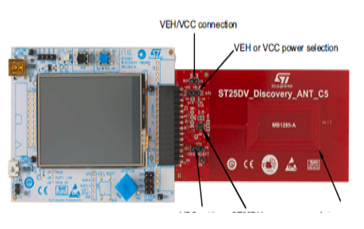
图5.MB1285板正面图
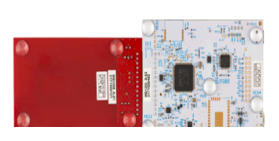
图6.MB1285板背面图
责任编辑:David
【免责声明】
1、本文内容、数据、图表等来源于网络引用或其他公开资料,版权归属原作者、原发表出处。若版权所有方对本文的引用持有异议,请联系拍明芯城(marketing@iczoom.com),本方将及时处理。
2、本文的引用仅供读者交流学习使用,不涉及商业目的。
3、本文内容仅代表作者观点,拍明芯城不对内容的准确性、可靠性或完整性提供明示或暗示的保证。读者阅读本文后做出的决定或行为,是基于自主意愿和独立判断做出的,请读者明确相关结果。
4、如需转载本方拥有版权的文章,请联系拍明芯城(marketing@iczoom.com)注明“转载原因”。未经允许私自转载拍明芯城将保留追究其法律责任的权利。
拍明芯城拥有对此声明的最终解释权。


 产品分类
产品分类






 2012- 2022 拍明芯城ICZOOM.com 版权所有 客服热线:400-693-8369 (9:00-18:00)


