


 产品分类
产品分类
Silicon Lab Si5338 I2C可编四时钟发生器解决方案
 133
133
 拍明
拍明
原标题:Silicon Lab Si5338 I2C可编四时钟发生器解决方案
Silicon Lab公司的Si5338是I2C可编任意频率任意输出的四个高性能低抖动时钟发生器,时钟频率高达350MHz,可选择频率高达710MHz,器件采用外接晶振支持自由运行操作,或锁住外接时钟产生同步时钟;输出驱动器支持四个差分时钟或八个单端时钟或两者的组合;输出驱动器可配置支持共同信号格式如LVPECL,LVDS,HCSL, CMOS, HSTL 和SSTL.单独输出电源引脚的电源可为3.3V,2.5V,1.8V和1.5V,支持多格式输出驱动器.核电压采用3.3V,2.5V或1.8V,并和输出电源分离.器件的相位抖动为0.7ps RMS,外接晶振为8-30MHz,CMOS输入频率为5-200 MHz,SSTL/HSTL输入频率为5-350 MHz,差分输入频率为5-710MHz,可配置输出频率LVPECL/LVDS为0.16-710 MHz,HCSL为0.16-250 MHz,CMOS为0.16-200 MHz,SSTL/HSTL为0.16-350 MHz.工作温度为–40到+85℃,主要用在以太网交换/路由器,PCIe Gen1/2/3/4,宽带视频/音频定时器,处理器和FPGA时钟,任意频率时钟转换,MSAN/DSLAM/PON,光纤通路,SAN,通信线路卡以及1 GbE和10 GbE.本文介绍了Si5338主要特性,功能框图,应用电路图以及Si5330/34/35/38评估板Si5338-EVB主要特性,框图,电路图,材料清单和PCB设计图.
The Si5338 is a high-performance, low-jitter clockgenerator capable of synthesizing four independentuser-programmable clock frequencies up to 350 MHzand select frequencies up to 710 MHz. The devicesupports free-run operation using an external crystal, orit can lock to an external clock for generatingsynchronous clocks. The output drivers support fourdifferential clocks or eight single-ended clocks or acombination of both. The output drivers are configurableto support common signal formats, such as LVPECL,LVDS, HCSL, CMOS, HSTL, and SSTL. Separateoutput supply pins allow supply voltages of 3.3, 2.5, 1.8,and 1.5 V to support the multi-format output driver. Thecore voltage supply accepts 3.3, 2.5, or 1.8 V and isindependent from the output supplies.
Using its two-stage synthesis architecture and patentedhigh-resolution MultiSynth technology, the Si5338 cangenerate four independent frequencies from a singleinput frequency. In addition to clock generation, theinputs can bypass the synthesis stage enabling theSi5338 to be used as a high-performance clock buffer ora combination of a buffer and generator.
For applications that need fine frequency adjustments,such as clock margining, each of the synthesizedfrequencies can be incremented or decremented inuser-defined steps as low as 1 ppm per step.
Output-to-output phase delays are also adjustable inuser-defined steps with an error of <20 ps tocompensate for PCB trace delays or for fine tuning ofsetup and hold margins.A zero-delay mode is also available to help minimizeinput-to-output delay. Spread spectrum is available oneach of the clock outputs for EMI-sensitive applications,such as PCI Express.
Configuration and control of the Si5338 is mainlyhandled through the I2C/SMBus interface. Somefeatures, such as output enable and frequency or phaseadjustments, can optionally be pin controlled. Thedevice has a maskable interrupt pin that can be monitored for loss of lock or loss of input signalconditions.
The device also provides the option of storing a userdefinableclock configuration in its non-volatile memory(NVM), which becomes the default clock configurationat power-up.
Si5338主要特性:
Low power MultiSynth™ technologyenables independent, any-frequencysynthesis on four differential outputdrivers
PCIe Gen 1/2/3/4 Common Clock andGen 3 SRNS compliant
Highly-configurable output drivers withup to four differential outputs, eight
single-ended clock outputs, or acombination of both
Low phase jitter of 0.7 ps RMS typ
High precision synthesis allows truezero ppm frequency accuracy on alloutputs
Flexible input reference:
External crystal: 8 to 30 MHz
CMOS input: 5 to 200 MHz
SSTL/HSTL input: 5 to 350 MHz
Differential input: 5 to 710 MHz
Independently configurable outputssupport any frequency or format:
LVPECL/LVDS: 0.16 to 710 MHz
HCSL: 0.16 to 250 MHz
CMOS: 0.16 to 200 MHz
SSTL/HSTL: 0.16 to 350 MHz
Independent output voltage per driver:1.5, 1.8, 2.5, or 3.3 V
Single supply core with excellentPSRR: 1.8, 2.5, 3.3 V
Independent frequency increment/decrement feature enablesglitchless frequency adjustments in1 ppm steps
Independent phase adjustment oneach of the output drivers with anaccuracy of <20 ps steps
Highly configurable spreadspectrum (SSC) on any output:
Any frequency from 5 to 350 MHz
Any spread from 0.5 to 5.0%
Any modulation rate from 33 to63 kHz
External feedback mode allowszero-delay mode
Loss of lock and loss of signalalarms
I2C/SMBus compatible interface
Easy to use programming software
Small size: 4 x 4 mm, 24-QFN
Low power: 45 mA core supply typ
Wide temperature range: –40 to+85℃
Si5338应用:
Ethernet switch/router
PCIe Gen1/2/3/4
Broadcast video/audio timing
Processor and FPGA clocking
Any-frequency clock conversion
MSAN/DSLAM/PON
Fibre Channel, SAN
Telecom line cards
1 GbE and 10 GbE

图1.Si5338功能框图

图2.Si5338典型应用电路图
Si5330/34/35/38评估板Si5338-EVB
The Si5338-EVB is used for evaluating the Si5330/34/35/38 family of any-frequency, any-output clockgenerators and clock buffers.
评估板Si5338-EVB主要特性:
Fully powered from a single USB port.
Onboard 25 MHz XTAL allows standaloneasynchronous operation on the Si5334/35/38.
GUI programmable VDD supply allows device tooperate from 3.3, 2.5, or 1.8 V.
GUI programmable VDDO supplies allow each of thefour outputs to have its own supply voltageselectable from 3.3, 2.5, 1.8, or 1.5 V
GUI-controlled voltage, current, and powermeasurements of VDD and all four VDDO supplies.
Voltage supply jumpers allow easy access for use ofexternal supplies or current measurements.
Input signal jumpers allow external control of pinfunctions such as output enable, phase inc/dec,frequency inc/dec, and I2C_LSB.

图3.评估板Si5338-EVB外形图

图4.评估板Si5338-EVB功能框图

图5.评估板Si5338-EVB主电路图

图6.评估板Si5338-EVB MCU电路图

图7.评估板Si5338-EVB电压稳压器电路图
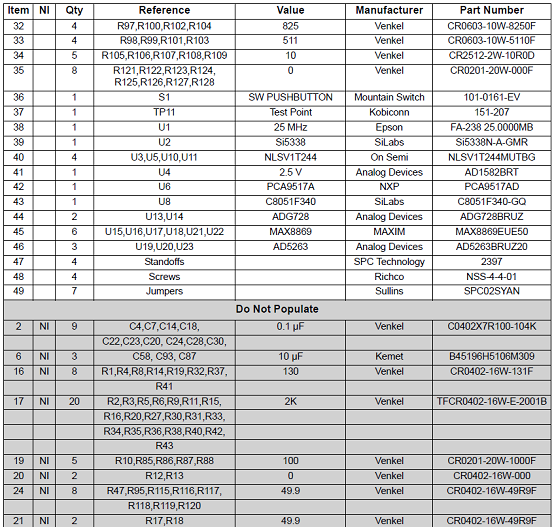
评估板Si5338-EVB材料清单:

责任编辑:David
【免责声明】
1、本文内容、数据、图表等来源于网络引用或其他公开资料,版权归属原作者、原发表出处。若版权所有方对本文的引用持有异议,请联系拍明芯城(marketing@iczoom.com),本方将及时处理。
2、本文的引用仅供读者交流学习使用,不涉及商业目的。
3、本文内容仅代表作者观点,拍明芯城不对内容的准确性、可靠性或完整性提供明示或暗示的保证。读者阅读本文后做出的决定或行为,是基于自主意愿和独立判断做出的,请读者明确相关结果。
4、如需转载本方拥有版权的文章,请联系拍明芯城(marketing@iczoom.com)注明“转载原因”。未经允许私自转载拍明芯城将保留追究其法律责任的权利。
拍明芯城拥有对此声明的最终解释权。
相关资讯
:
基于MC33771主控芯片的新能源锂电池管理系统解决方案

AMIC110 32位Sitara ARM MCU开发方案

基于AMIC110多协议可编程工业通信处理器的32位Sitara ARM MCU开发方案

基于展讯SC9820超低成本LTE芯片平台的儿童智能手表解决方案

基于TI公司的AM437x双照相机参考设计

基于MTK6580芯片的W2智能手表解决方案


 2012- 2022 拍明芯城ICZOOM.com 版权所有 客服热线:400-693-8369 (9:00-18:00)


