


 产品分类
产品分类
NXP KW36Z超低功耗无线BLE和FSK MCU解决方案
 199
199
 拍明
拍明
原标题:NXP KW36Z超低功耗无线BLE和FSK MCU解决方案
摘要: nxp公司的KW36Z/35Z是超低功耗高度集成的无线MCU,基于ARM CortexR-M0+核,具有蓝牙低功耗(BLE)和通用FSK连接.器件还集成了多达512KB闪存和64KB SRAM以及支持BLE 5.0和通用FSK调制的2.4GHz无线电;此外KW36Z还集成了能无缝连接工业CAN通信网络的FlexCAN模块,支持CAN灵活的数据速率(CAN FD)协议,以满足宽带宽和低等待的需求.主要用在工业控制,医疗/健康等嵌入系统.本文介绍了KW36Z/35Z主要特性,框图和主要特性,包办无线电特性,MCU特性和外设等,以及开发板FRDM-KW36主要特性,框图和电路图.
The KW36Z/35Z wireless microcontrollers (MCU), which includes the KW36Z and KW35Z families of devices, are highly integrated single-chip devices that enable Bluetooth Low Energy (BLE) and Generic FSK connectivity for industrial and medical/ healthcare embedded systems. The target applications center on wirelessly bridging the embedded world with mobile devices to enhance the human interface experience, share embedded data between devices and the cloud and enable wireless firmware updates.
The KW36Z/35Z Wireless MCU integrates an Arm? Cortex?-M0+ CPU with up to 512 KB flash and 64 KB SRAM and a 2.4 GHz radio that supports BLE 5.0 and Generic FSK modulations. The BLE radio supports up to 8 simultaneous connections in any master/slave combination. The Medical Body Area Network (MBAN) frequencies from 2.36 to 2.4 GHz are also supported enabling wearable or implantable wireless medical devices.
The KW36Z includes an integrated FlexCAN module enabling seamless integration into an industrial CAN communication network, enabling communication with external control and sensor monitoring devices over BLE. The FlexCAN module can support CAN’s flexible data-rate (CAN FD) protocol for increased bandwidth and lower latency.
The KW36Z/35Z devices can be used as a "BlackBox" modem in order to add BLE or Generic FSK connectivity to an existing host MCU or MPU (microprocessor), or may be used as a standalone smart wireless sensor with embedded application where no host
controller is required.
The RF circuit of the KW36Z/35Z is optimized to require very few external components, achieving the smallest RF footprint possible on a printed circuit board.
Extremely long battery life is achieved through the efficiency of code execution in the
Cortex-M0+ CPU core and the multiple low power operating modes of the KW36Z/35Z. For power critical applications, an integrated DC-DC converter enables operation from a single coin cell or Li-ion battery with a significant reduction of peak receive and transmit current consumption.
KW36Z主要特性:
Multi-Standard Radio
• 2.4 GHz Bluetooth Low Energy version 5.0 compliant supporting up to 8 simultaneous hardware connections
• Generic FSK modulation
• Data Rate: 250, 500 and 1000 kbps
• Modulations: GFSK BT = 0.3, 0.5, and 0.7;
FSK/MSK
• Modulation Index: 0.32, 0.5, 0.7, and 1.0
• Typical Receiver Sensitivity (BLE 1 Mbps) = -95 dBm
• Typical Receiver Sensitivity (250 kbps GFSK-BT=0.5, h=0.5) = -99 dBm
• Programmable Transmitter Output Power: -30 dBm to +3.5 dBm
• Low external component counts for low cost application
• On-chip balun with single ended bidirectional RF port
MCU and Memories
• 256 KB program flash memory plus 256 KB FlexNVM on KW36Z
• 8 KB FlexRAM supporting EEPROM emulation on KW36Z
• 512 KB program flash memory on KW35Z
• Up to 48 MHz ArmR CortexR-M0+ core
• On-chip 64 KB SRAM
Low Power Consumption
• Transceiver current (DC-DC buck mode, 3.6 V supply)
• Typical Rx Current: 6.3 mA
• Typical Tx current: 5.7 mA (0 dBm output)
• Low Power Mode (VLLS0) Current: 258 nA
System peripherals
• Nine MCU low-power modes to provide power optimization based on application requirements
• DC-DC Converter supporting Buck and Bypass operating modes
• Direct memory access (DMA) Controller
• Computer operating properly (COP) watchdog
• Serial wire debug (SWD) Interface and Micro Trace buffer
• Bit Manipulation Engine (BME)
Analog Modules
• 16-bit Analog-to-Digital Converter (ADC)
• 6-bit High Speed Analog Comparator (CMP)
• 1.2 V voltage reference (VREF)
Timers
• 16-bit low-power timer (LPTMR)
• 3 Timer/PWM Modules(TPM): One 4 channel TPM and two 2 channel TPMs
• Programmable Interrupt Timer (PIT)
• Real-Time Clock (RTC)
Communication interfaces
• 2 serial peripheral interface (SPI) modules
• 2 inter-integrated circuit (I2C) modules
• Low Power UART (LPUART) module with LIN support (2x LPUART on KW36Z)
• Carrier Modulator Timer (CMT)
• FlexCAN module (with CAN FD support up to 3.2 Mbps baudrate) on KW36Z
Clocks
• 26 and 32 MHz supported for BLE and Generic FSK modes
• 32.768 kHz Crystal Oscillator
Operating Characteristics
• Voltage range: 1.71 V to 3.6 V
• Ambient temperature range: –40 to 105 °C
• Industrial Qualification
Human-machine interface
• General-purpose input/output
Security
• AES-128 Hardware Accelerator (AESA)
• True Random Number Generator (TRNG)
• Advanced flash security on Program Flash
• 80-bit unique identification number per chip
• 40-bit unique media access control (MAC) subaddress
• LE Secure Connections
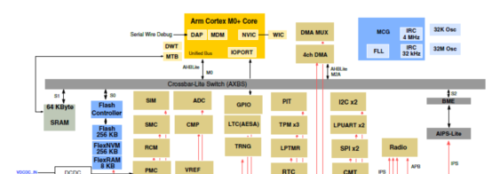
图1.KW36框图
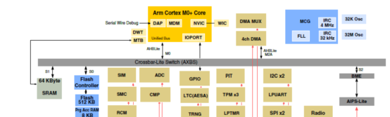
图2.KW35框图
无线电特性:
Radio features
• 2.4 GHz ISM band (2400-2483.5 MHz)
• Medical Body Area Network (MBAN) 2360-2400 MHz
Supported standards:
• Bluetooth Low Energy Version 5 compliant radio
• Generic FSK modulation supporting data rates up to 1 Mbps
• Support for up to 8 simultaneous BLE hardware connections in any master, slave
combination
• Bluetooth Low Energy(BLE) Application Profiles
Receiver performance:
• Receive sensitivity of up to -95 dBm for BLE
• Receive sensitivity of up to -99 dBm for a 250 kbps GFSK mode with a modulation
index of 0.5. Receive sensitivity in Generic FSK modes depends on mode selection
and data rate.
Other features:
• Programmable transmit output power from -30 dBm to +3.5 dBm
• Integrated on-chip balun
• Single ended bidirectional RF port shared by transmit and receive
• Low external component count
• Supports transceiver range extension using external PA and/or LNA
• 26 MHz and 32 MHz crystals supported for BLE and Generic FSK modes
• Bluetooth Low Energy version 5 Link Layer hardware with 1 Mbps PHY support
• Hardware acceleration for Generic FSK packet processing
• Generic FSK modulation at 250, 500 and 1000 kbps
• Supports 8 simultaneous BLE connections in any master/slave combination
• Enhanced BLE automatic deep sleep modes (DSM) supporting Slave Latency
• Up to 26 devices supported by whitelist in hardware
• Up to 8 private resolvable addresses supported in hardware
• Supports DMA capture of IQ data with sampling rate of up to 2 MHz, when using a 32 MHz crystal
MCU特性:
Arm Cortex-M0+ CPU
• Up to 48 MHz CPU
• As compared to Cortex-M0, the Cortex-M0+ uses an optimized 2-stage pipeline
microarchitecture for reduced power consumption and improved architectural
performance (cycles per instruction)
• Supports up to 32 interrupt request sources
• Binary compatible instruction set architecture with the Cortex-M0 core
• Thumb instruction set combines high code density with 32-bit performance
• Serial Wire Debug (SWD) reduces the number of pins required for debugging
• Micro Trace Buffer (MTB) provides lightweight program trace capabilities using system RAM as the destination memory
Nested Vectored Interrupt Controller (NVIC)
• 32 vectored interrupts, 4 programmable priority levels
• Includes a single non-maskable interrupt
Wake-up Interrupt Controller (WIC)
• Supports interrupt handling when system clocking is disabled in low power modes
• Takes over and emulates the NVIC behavior when correctly primed by the NVIC
on entry to very-deep-sleep
• A rudimentary interrupt masking system with no prioritization logic signals for wake-up as soon as a non-masked interrupt is detected
Debug Controller
• Two-wire Serial Wire Debug (SWD) interface
• Hardware breakpoint unit for 2 code addresses
• Hardware watchpoint unit for 2 data items
• Micro Trace Buffer for program tracing
On-Chip Memory
• Up to 512 KB Flash
• KW36Z contains 256 KB program flash with ECC and 256 KB FlexNVM.
• KW35Z contains 512 KB program flash with ECC.
• Flash implemented as two equal blocks each of 256 KB block. Code can execute or read from one block while the other block is being erased or programmed on KW35Z only.
• Firmware distribution protection. Program flash can be marked execute-only on a per-sector (8 KB) basis to prevent firmware contents from being read by third parties.
• 64 KB SRAM
• KW36Z contains 8 KB FlexRAM.
• KW35Z contains 8 KB program acceleration RAM.
• Security circuitry to prevent unauthorized access to RAM and flash contents through the debugger
系统特性:
Power Management Control Unit (PMC)
• Programmable power saving modes
• Available wake-up from power saving modes via internal and external sources
• Integrated Power-on Reset (POR)
• Integrated Low Voltage Detect (LVD) with reset (brownout) capability
• Selectable LVD trip points
• Programmable Low Voltage Warning (LVW) interrupt capability
• Individual peripheral clocks can be gated off to reduce current consumption
• Internal Buffered bandgap reference voltage
• Factory programmed trim for bandgap and LVD
• 1 kHz Low Power Oscillator (LPO)
DC-DC Converters
• Internal switched mode power supply supporting Buck and Bypass operating
modes
• Buck operation supports external voltage sources of 2.1 V to 3.6 V
• When DC-DC is not used, the device supports an external voltage range of 1.5 V to
3.6 V (1.5 - 3.6 V on VDD_RF1, VDD_RF2, VDD_XTAL and
VDD_1P5OUT_PMCIN pins. 1.71 - 3.6 V on VDD_0, VDD_1 and VDDA pins)
• An external inductor is required to support the Buck mode
• The DC-DC Converter VDD_1P8OUT current drive for external devices (MCU in
RUN mode, Radio is enabled, other peripherals are disabled)
• Up to 44 mA in buck mode with VDD_1P8OUT = 1.8 V
• Up to 31.4 mA in buck mode with VDD_1P8OUT = 3.0 V
Direct Memory Access (DMA) Controller
• All data movement via dual-address transfers: read from source, write to destination
• Programmable source and destination addresses and transfer size
• Support for enhanced addressing modes
• 4-channel implementation that performs complex data transfers with minimal intervention from a host processor
• Internal data buffer, used as temporary storage to support 16- and 32-byte transfers
• Connections to the crossbar switch for bus mastering the data movement
• Transfer control descriptor (TCD) organized to support two-deep, nested transfer
operations
• 32-byte TCD stored in local memory for each channel
• An inner data transfer loop defined by a minor byte transfer count
• An outer data transfer loop defined by a major iteration count
• Channel activation via one of three methods:
• Explicit software initiation
• Initiation via a channel-to-channel linking mechanism for continuous transfers
• Peripheral-paced hardware requests, one per channel
• Fixed-priority and round-robin channel arbitration
• Channel completion reported via optional interrupt requests
• One interrupt per channel, optionally asserted at completion of major iteration count
• Optional error terminations per channel and logically summed together to form one error interrupt to the interrupt controller
• Optional support for scatter/gather DMA processing
• Support for complex data structures
DMA Channel Multiplexer (DMA MUX)
• 4 independently selectable DMA channel routers
• 2 periodic trigger sources available
• Each channel router can be assigned to 1 of the peripheral DMA sources
COP Watchdog Module
• Independent clock source input (independent from CPU/bus clock)
• Choice between two clock sources
• LPO oscillator
• Bus clock
System Clocks
• Both 26 MHz and 32 MHz crystal reference oscillator supported for BLE and Generic FSK modes
• MCU can derive its clock either from the crystal reference oscillator or the frequency locked loop (FLL)1
• 32.768 kHz crystal reference oscillator used to maintain precise Bluetooth Low Energy timing in low power modes
• Multipurpose Clock Generator (MCG)
• Internal reference clocks — Can be used as a clock source for other on-chip peripherals
• On-chip RC oscillator range of 31.25 kHz to 39.0625 kHz with 2% accuracy across full temperature range
• On-chip 4 MHz oscillator with 5% accuracy across full temperature range
• Frequency-locked loop (FLL) controlled by internal or external reference
• 20 MHz to 48 MHz FLL output
Unique Identifiers
• 80-bit Unique ID represents a unique identifier for each chip
• 40-bit unique Media Access Control (MAC) address, which can be used to build a
unique 48-bit Bluetooth Low Energy MAC address
Peripheral features
16-bit Analog-to-Digital Converter (ADC)
• Linear successive approximation algorithm with 16-bit resolution
• Output formatted in differential-ended 16-, 13-, 11-, and 9-bit mode
• Output formatted in single-ended 16-, 12-, 10-, and 8-bit mode
• Single or continuous conversion
• Configurable sample time and conversion speed / power
• Conversion rates in 16-bit mode with no averaging up to ~500Ksamples/sec
• Input clock selection
• Operation in low power modes for lower noise operation
• Asynchronous clock source for lower noise operation
• Selectable asynchronous hardware conversion trigger
• Automatic compare with interrupt for less-than, or greater than, or equal to programmable value
• Temperature sensor
• Battery voltage measurement
• Hardware average function
• Selectable voltage reverence
• Self-calibration mode
High-Speed Analog Comparator (CMP)
• 6-bit DAC programmable reference generator output
• Up to eight selectable comparator inputs; each input can be compared with any input by any polarity sequence
• Selectable interrupt on rising edge, falling edge, or either rising or falling edges of comparator output
• Two performance modes:
• Shorter propagation delay at the expense of higher power
• Low power, with longer propagation delay
• Operational in all MCU power modes except VLLS0 mode
Voltage Reference(VREF1)
• Programmable trim register with 0.5 mV steps, automatically loaded with factory trimmed value upon reset
• Programmable buffer mode selection:
• Off
• Bandgap enabled/standby (output buffer disabled)
• High power buffer mode (output buffer enabled)
• 1.2 V output at room temperature
• VREF_OUT output signal
Low Power Timer (LPTMR)
• One channel
• Operation as timer or pulse counter
• Selectable clock for prescaler/glitch filter
• 1 kHz internal LPO
• External low power crystal oscillator
• Internal reference clock
• Configurable glitch filter or prescaler
• Interrupt generated on timer compare
• Hardware trigger generated on timer compare
• Functional in all power modes
Timer/PWM (TPM)
• TPM0: 4 channels, TPM1 and TPM2: 2 channels each
• Selectable source clock
• Programmable prescaler
• 16-bit counter supporting free-running or initial/final value, and counting is up or up-down
• Input capture, output compare, and edge-aligned and center-aligned PWM modes
• Input capture and output compare modes
• Generation of hardware triggers
• TPM1 and TPM2: Quadrature decoder with input filters
• Global time base mode shares single time base across multiple TPM instances
Programmable Interrupt Timer (PIT)
• Up to 2 interrupt timers for triggering ADC conversions
• 32-bit counter resolution
• Clocked by bus clock frequency
Real-Time Clock (RTC)
• 32-bit seconds counter with 32-bit alarm
• Can be invalidated on detection of tamper detect
• 16-bit prescaler with compensation
• Register write protection
• Hard Lock requires MCU POR to enable write access
• Soft lock requires POR or software reset to enable write/read access
• Capable of waking up the system from low power modes
Inter-Integrated Circuit (I2C)
• Two channels
• Compatible with I2C bus standard and SMBus Specification Version 2 features
• Up to 400 kHz operation
• Multi-master operation
• Software programmable for one of 64 different serial clock frequencies
• Programmable slave address and glitch input filter
• Interrupt driven byte-by-byte data transfer
• Arbitration lost interrupt with automatic mode switching from master to slave
• Calling address identification interrupt
• Bus busy detection broadcast and 10-bit address extension
• Address matching causes wake-up when processor is in low power mode
LPUART
• One channel (2 channels on KW36Z)
• Full-duplex operation
• Standard mark/space non-return-to-zero (NRZ) format
• 13-bit baud rate selection with fractional divide of 32
• Programmable 8-bit or 9-bit data format
• Programmable 1 or 2 stop bits
• Separately enabled transmitter and receiver
• Programmable transmitter output polarity
• Programmable receive input polarity
• 13-bit break character option
• 11-bit break character detection option
• Two receiver wakeup methods:
• Idle line wakeup
• Address mark wakeup
• Address match feature in receiver to reduce address mark wakeup ISR overhead
• Interrupt or DMA driven operation
• Receiver framing error detection
• Hardware parity generation and checking
• Configurable oversampling ratio to support from 1/4 to 1/32 bit-time noise detection
• Operation in low power modes
• Hardware Flow Control RTSCTS
• Functional in Stop/VLPS modes
• Break detect supporting LIN
Serial Peripheral Interface (SPI)
• Two independent SPI channels
• Master and slave mode
• Full-duplex, three-wire synchronous transfers
• Programmable transmit bit rate
• Double-buffered transmit and receive data registers
• Serial clock phase and polarity options
• Slave select output
• Control of SPI operation during wait mode
• Selectable MSB-first or LSB-first shifting
• Support for both transmit and receive by DMA
Carrier Modulator Timer (CMT)
• Four modes of operation
• Time; with independent control of high and low times
• Baseband
• Frequency shift key (FSK)
• Direct software control of CMT_IRO signal
• Extended space operation in time, baseband, and FSK modes
• Selectable input clock divider
• Interrupt on end of cycle
• Ability to disable CMT_IRO signal and use as timer interrupt
General Purpose Input/Output (GPIO)
• Hysteresis and configurable pull up device on all input pins
• Independent pin value register to read logic level on digital pin
• All GPIO pins can generate IRQ and wakeup events
• Configurable drive strength on some output pins
• GPIO can be configured to function as a interrupt driven keyboard scanning matrix
• In the 48-pin package there are a total of 25 digital pins
• In the 40-pin package there are a total of 18 digital pins
FlexCAN (for KW36Z only)
• Full implementation of the CAN with Flexible Data Rate (CAN FD) protocol specification and CAN protocol specification, Version 2.0 B
• Flexible Message Buffers (MBs); there are total 32 MBs of 8 bytes data length each, configurable as Rx or Tx, all supporting standard and extended messages
• Programmable clock source to the CAN Protocol Interface, either peripheral clock or oscillator clock
• Capability to select priority between mailboxes and Rx FIFO during matching process
• Powerful Rx FIFO ID filtering, capable of matching incoming IDs against either 128 extended, 256 standard, or 512 partial (8 bit) IDs, with up to 32 individual masking capability
Key Specifications
KW36Z/35Z meets or exceeds all Bluetooth Low Energy version 5 performance specifications. The key specification for the KW36Z/35Z are:
Frequency Band:
• ISM Band: 2400 to 2483.5 MHz
• MBAN Band: 2360 to 2400 MHz
Bluetooth Low Energy version 5 modulation scheme:
• Symbol rate: 1000 kbps
• Modulation: GFSK
• Receiver sensitivity: -95 dBm, typical
• Programmable transmitter output power: -30 dBm to +3.5 dBm
Generic FSK modulation scheme:
• Symbol rate: 250, 500 and 1000 kbps
• Modulation(s): GFSK (modulation index = 0.32, 0.5, 0.7 and 1.0, BT =0.3, 0.5, and 0.7), FSK and MSK
• Receiver Sensitivity: Mode and data rate dependent. -99 dBm typical for GFSK (r=250 kbps, BT = 0.5, h = 0.5)
FRDM-KW36 Freedom Development Board
开发板FRDM-KW36
This guide describes the hardware for the FRDM-KW36 Freedom development board. The FRDM-KW36 Freedom development board is highly configurable, low-power, and cost-effective evaluation board for application prototyping and demonstration of the KW36A/35A and KW36Z/35Z family of devices. This evaluation board offers easy-to-use mass-storage-device mode flash programmer, a virtual serial port, and standard programming and run-control capabilities.
The KW36 is an ultra-low-power, highly integrated single-chip device that enables Bluetooth® Low Energy (LE) or Generic FSK (at 250, 500 and 1000 kbps) for portable, low-power embedded systems.
The KW36 integrates a radio transceiver operating in the 2.36 GHz to 2.48 GHz range supporting a range of GFSK, an Arm Cortex-M0+ CPU, up to 512 KB Flash and up to 64 KB SRAM, Bluetooth LE Link Layer hardware and peripherals optimized to meet the requirements of the target applications.
The FRDM-KW36 development board is an evaluation environment supporting KW35Z/36Z/35A/36A (KW36) Wireless Microcontrollers (MCU). The KW36 integrates a radio transceiver operating in the 2.4 GHz band (supporting a range of GFSK and Bluetooth LE) and an Arm Cortex-M0+ MCU into a single package. NXP supports the KW36 with tools and software that include hardware evaluation and development boards, software development IDE, applications, drivers, and a custom PHY with a Bluetooth LE Link Layer. The FRDM-KW36 development board consists of the KW36Z device with a 32 MHz reference crystal oscillator, RF circuitry (including antenna), 4-Mbit external serial flash, CAN and LIN transceivers and supporting circuitry in the popular Freedom board form-factor. The board is a standalone PCB and supports application development with NXP’s Bluetooth LE and Generic FSK libraries.
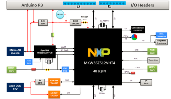
图3. 开发板FRDM-KW36框图
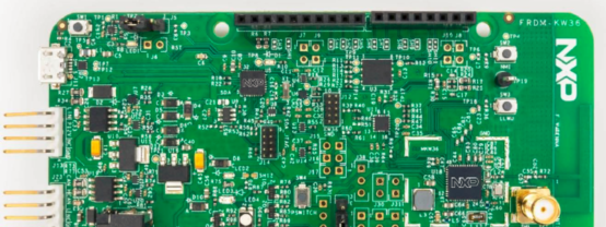
图4. 开发板FRDM-KW36外形图
开发板FRDM-KW36主要特性:
• NXP ultra-low-power KW36Z Wireless MCU supporting Bluetooth LE and Generic FSK.
• Compliant Bluetooth 5 LE.
• Reference design area with small-footprint, low-cost RF node:
— Single-ended input/output port.
— Low count of external components.
— Programmable output power from -30 dBm to +3.5 dBm at the SMA connector, when using DCDC Bypass or operating the DCDC in Buck mode.
— Receiver sensitivity is -100 dBm, typical (@1 % PER for 20-byte payload packet) for GFSK applications (250 kbps, BT=0.5, h=0.5), at the SMA connector.
— Receiver sensitivity is -95 dBm (for Bluetooth LE applications) at the SMA connector.
• Integrated PCB inverted F-type antenna and SMA RF port (requires moving C55 to C57)
• Selectable power sources.
• DC-DC converter with Buck, and Bypass operation modes.
• 32 MHz reference oscillator for RF operation.
• 32.768 kHz reference oscillator mainly used for RTC operation and RF low power operation.
• 2.4 GHz frequency operation (ISM and MBAN).
• 4-Mbit (512 kB) external serial flash memory for Over-The-Air Programming (OTAP) support
• NXP FXOS8700CQ Digital Sensor, 3D Accelerometer (±2g/±4g/±8g) + 3D Magnetometer
• Thermistor circuit to test KW36 ADC module.
• Coin cell connector compatible with a CR2032 coin cell. CAN/LIN transceivers are not functional when using coin cell.
• Integrated Open-Standard Serial and Debug Adapter (OpenSDA).
• Cortex 10-pin (0.05″) SWD debug port for target MCU.
• Cortex 10-pin (0.05″) JTAG port for OpenSDA updates.
• One RGB LED indicator.
• One red LED indicator.
• Two push-button switches.
• NXP TJA1057 high-speed CAN transceiver.
• NXP TJA1027 LIN 2.2A/SAE J2602 transceiver.
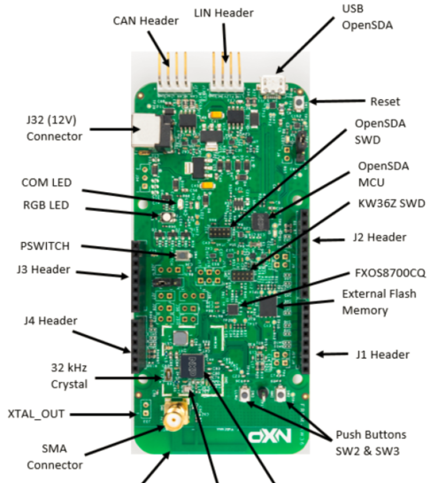
图5. 开发板FRDM-KW36元件配置图
责任编辑:David
【免责声明】
1、本文内容、数据、图表等来源于网络引用或其他公开资料,版权归属原作者、原发表出处。若版权所有方对本文的引用持有异议,请联系拍明芯城(marketing@iczoom.com),本方将及时处理。
2、本文的引用仅供读者交流学习使用,不涉及商业目的。
3、本文内容仅代表作者观点,拍明芯城不对内容的准确性、可靠性或完整性提供明示或暗示的保证。读者阅读本文后做出的决定或行为,是基于自主意愿和独立判断做出的,请读者明确相关结果。
4、如需转载本方拥有版权的文章,请联系拍明芯城(marketing@iczoom.com)注明“转载原因”。未经允许私自转载拍明芯城将保留追究其法律责任的权利。
拍明芯城拥有对此声明的最终解释权。
相关资讯
:
基于MC33771主控芯片的新能源锂电池管理系统解决方案

AMIC110 32位Sitara ARM MCU开发方案

基于AMIC110多协议可编程工业通信处理器的32位Sitara ARM MCU开发方案

基于展讯SC9820超低成本LTE芯片平台的儿童智能手表解决方案

基于TI公司的AM437x双照相机参考设计

基于MTK6580芯片的W2智能手表解决方案


 2012- 2022 拍明芯城ICZOOM.com 版权所有 客服热线:400-693-8369 (9:00-18:00)


