On Semi AXM0F243超低功耗PowerRFMCU开发方案
 233
233
 拍明
拍明
原标题:On Semi AXM0F243超低功耗PowerRFMCU开发方案
On Semi公司的AXM0F243真正单片无线应用的系统级芯片(SoC), RF载频为27-1050MHz,包括现场验证过的窄带AX5043 RF收发器核和高性能ARM® Cortex®-M0+微控制器核. AX5043核功能极为强大,软件可编程.具有最宽阵列可用调制方案,数据速率从100bps到125kbps,几乎可以实现基于专有或标准的任何亚GHz协议.无线电核的软件可编程性也使它能共享有不同软件加载的产品的共通硬件设计,使用户方便地管理多个SKU.采用该器件也能实现多协议解决方案,以实现功能强大的网关.AX5043接收器灵敏度低至-137 dBm,而功耗小于10mA,AX5043发送器包括差分功率放大器,可产生高达16dBm功率,如选择单端工作则可产生高达13dBm功率.高性能ARM® Cortex®-M0+核工作频率高达48MHz,有64KB闪存和8KB RAM,MCU包含两个单独的串行通信区块,可以配置成I2C,SPI,UART等.MCU还有五个16位计时器,能用作计数器,PWM调制器,或脉冲发生器.有19个可编程GPIO引脚.主要用在物联网,自动读表(AMR),安全应用,建筑物自动化,无线网络和信息传呼.本文介绍了AXM0F243主要特性,框图和多种应用框图,以及评估板DVK−AXM0F243−868−x−GEVK套件主要特性,电路图,材料清单和PCB设计图.
The AXM0F243 is a System on Chip (Soc) for true single chip wireless applications. The SoC contains the field proven narrow-band AX5043 RF transceiver core and a high performance ARM® Cortex®-M0+ microcontroller (MCU) core.
The AX5043 core is extremely powerful and is software programmable. With the widest array of available modulation schemes and data rates from 100 bps to 125 kbps, nearly any Sub GHz protocol, proprietary or standards based, can be implemented.
The software programmability of the radio core also makes it possible to share a common hardware design for products that have different software loaded, making it easier for customers to manage multiple SKUs. It’s also possible to implement a multi-protocol solution using this device for powerful gateway implementations.
The integrated frequency synthesizer can generate any carrier frequency from 27 MHz to 1050 MHz. For frequencies below ~400 MHz an external inductor is used by the integrated VCO, but above ~400 MHz an integrated inductor can be used instead.
The AX5043 receiver is extremely robust and can achieve sensitivities as low as -137 dBm, while consuming less than 10 mA of current. For applications that require antenna diversity, an integrated diversity controller is included and can automatically control an external antenna switch through a GPIO pin. The receiver also has a wake on radio feature, which further reduces power consumption by allowing the MCU to sleep as long and as often as possible between radio events.
The AX5043 transmitter includes either a differential power amplifier that generates up to 16 dBm or a single ended option for up to 13 dBm.
The high performance ARM® Cortex®-M0+ runs at up to 48 MHz and has 64 kB of FLASH and 8 kB of RAM. The MCU contains two independent serial communication blocks (SCBs) which can be configured to do I2C, SPI, UART, etc. The MCU has five 16 bit timers that act as counters, PWM modulators, or pulse generators. There are 19 programmable GPIO pins.
In addition to the extremely powerful MCU core, the AXM0F243 MCU also has powerful and unique analog functionality. There is an integrated 12 bit SAR ADC capable of 1 Mspsconversions, with single-ended and fully differential modes. The MCU also contains two current DACs, two ultra-low power comparators and two ultra-low power operational amplifiers.
With its robust and efficient RF transceiver, and powerful ARM® Cortex®-M0+ MCU and programmable analog, the AXM0F243 is an outstanding choice for low power and long range Internet of Things applications.
AXM0F243主要特性:
System−on−Chip (SoC) Ultra−low Power AdvancedNarrow−band RF−microcontroller for WirelessCommunication Applications
• QFN40 Package
• Supply Range 1.8 V − 3.6 V
• −40℃ to 85℃
• Deep Sleep Mode with Operational Analog and 2.5 _ADigital System Current
• Radio RX−mode
6.5 mA @ 169 MHz
9.5 mA @ 868 MHz and 433 MHz
• Radio TX−mode at 868 MHz
7.6 mA @ 0 dBm
21 mA @ 10 dBm
55 mA @ 15 dBm
• This is a Pb−Free Device
32−bit MCU Subsystem
• 48−MHz ARM Cortex−M0+ CPU
• Up to 64 KB of Flash with Read Accelerator
• Up to 8 KB of SRAM
Programmable Analog
• Two opamps with reconfigurable high−drive externaland high−bandwidth internal drive and Comparatormodes and ADC input buffering capability. Opampscan operate in Deep Sleep low−power mode.
• 12−bit 1−Msps SAR ADC with differential andsingle−ended modes
• Single−slope 10−bit ADC function
• Two current DACs (IDACs) for general−purposeapplications on any pin
• Two low−power comparators that operate in DeepSleep low−power mode
Programmable Digital
• Programmable logic blocks allowing Booleanoperations to be performed on port inputs and outputs
Low−Power 1.8 V to 3.6 V Operation
• Deep Sleep mode with operational analog and 2.5 _Adigital system current
Serial Communication
• Two independent run−time reconfigurable SerialCommunication Blocks (SCBs) with re−configurableI2C, SPI, or UART functionality
Timing and Pulse−Width Modulation
• Five 16−bit timer/counter/pulse−width modulator(TCPWM) blocks
• Center−aligned, Edge, and Pseudo−random modes
• Comparator−based triggering of Kill signals for motordrive and other high−reliability digital logicapplications
Up to 19 Programmable GPIO Pins
• Any GPIO pin can be analog, or digital
• Drive modes, strengths, and slew rates areProgrammableHigh Performance Narrow−band RF Transceivercompatible to AX5043 (FSK/MSK/4−FSK/GFSK/GMSK/
ASK/AFSK/FM/PSK)
• Receiver
♦ Carrier Frequencies from 27 to 1050 MHz
♦ Data Rates from 0.1 kbps to 125 kbps
♦ Optional Forward Error Correction (FEC)
♦ Sensitivity without FEC
−135 dBm @ 0.1 kbps, 868 MHz, FSK
−126 dBm @ 1 kbps, 868 MHz, FSK
−117 dBm @ 10 kbps, 868 MHz, FSK
−107 dBm @ 100 kbps, 868 MHz, FSK
−105 dBm @ 125 kbps, 868 MHz, FSK
−138 dBm @ 0.1 kbps, 868 MHz, PSK
−130 dBm @ 1 kbps, 868 MHz, PSK
−120 dBm @ 10 kbps, 868 MHz, PSK
−109 dBm @ 100 kbps, 868 MHz, PSK
−108 dBm @ 125 kbps, 868 MHz, PSK
♦ Sensitivity with FEC
−137 dBm @ 0.1 kbps, 868 MHz, FSK
−122 dBm @ 5 kbps, 868 MHz, FSK
−111 dBm @ 50 kbps, 868 MHz, FSK
♦ High Selectivity Receiver with up to 47 dB AdjacentChannel Rejection
♦ 0 dBm Maximum Input Power
♦ ±10% Data−rate Error Tolerance
♦ Support for Antenna Diversity with ExternalAntenna Switch
♦ Short Preamble Modes allow the Receiver to workwith as little as 16 Preamble Bits
♦ Fast State Switching Times
200 _s TX → RX Switching Time
62 _s RX → TX Switching Time
• Transmitter
♦ Carrier Frequencies from 27 to 1050 MHz
♦ Data−rates from 0.1 kbps to 125 kbps
♦ High Efficiency, High Linearity Integrated PowerAmplifier
♦ Maximum Output Power
16 dBm @ 868 MHz
16 dBm @ 433 MHz
16 dBm @ 169 MHz
♦ Power Level programmable in 0.5 dB Steps
♦ GFSK Shaping with BT=0.3 or BT=0.5
♦ Unrestricted Power Ramp Shaping
• RF Frequency Generation
♦ Configurable for Usage in 27 MHz −1050 MHzBands
♦ RF Carrier Frequency and FSK DeviationProgrammable in 1 Hz Steps
♦ Ultra Fast Settling RF Frequency Synthesizer forLow−power Consumption
♦ Fully Integrated RF Frequency Synthesizer withVCO Auto−ranging and Band−width Boost Modesfor Fast Locking
♦ Configurable for either Fully Integrated VCO,Internal VCO with External Inductor or FullyExternal VCO
♦ Configurable for either Fully Integrated or ExternalSynthesizer Loop Filter for a Large Range ofBandwidths
♦ Channel Hopping up to 2000 hops/s
♦ Automatic Frequency Control (AFC)
• Flexible Antenna Interface
♦ Integrated RX/TX Switching with DifferentialAntenna Pins
♦ Mode with Differential RX Pins and Single−endedTX Pin for Usage with External PAs and forMaximum PA Efficiency at Low Output Power
• Wakeup−on−Radio
♦ 640 Hz or 10 kHz Lowest Power Wake−up Timer
♦ Wake−up Time Interval programmable between98 _s and 102 s
• Sophisticated Radio Controller
♦ Antenna Diversity and RX/TX Switch Control
♦ Fully Automatic Packet Reception and Transmissionwithout Micro−controller Intervention
♦ Supports HDLC, Raw, Wireless M−Bus Frames andArbitrary Defined Frames
♦ Automatic Channel Noise Level Tracking
♦ _s Resolution Timestamps for Exact Timing (eg. ForFrequency Hopping Systems)
♦ 256 Byte Micro−programmable FIFO, optionallysupports Packet Sizes > 256 Bytes
♦ Three Matching Units for Preamble Byte,Sync−word and Address
♦ Ability to store RSSI, Frequency Offset andData−rate Offset with the Packet Data
♦ Multiple Receiver Parameter Sets allow the use ofmore aggressive Receiver Parameters duringPreamble, dramatically shortening the RequiredPreamble Length at no Sensitivity Degradation
• Advanced Crystal Oscillator (RF Reference Oscillator)
♦ Fast Start−up and Lowest Power Steady−state XTALOscillator for a Wide Range of Crystals
♦ Integrated Tuning Capacitors
♦ Possibility of Applying an External Clock Reference(TCXO)
AXM0F243应用:
27 − 1050 MHz Licensed and Unlicensed Radio Systems
• Internet of Things
• Automatic meter reading (AMR)
• Security applications
• Building automation
• Wireless networks
• Messaging Paging
• Compatible with: Wireless M−Bus, POCSAG, FLEX,KNX, Sigfox, Z−Wave, enocean
• Regulatory Regimes: EN 300 220 V2.3.1 including theNarrow−band 12.5 kHz, 20 kHz and 25 kHzDefinitions; EN 300 422; FCC Part 15.247; FCC Part15.249; FCC Part 90 6.25 kHz, 12.5 kHz and 25 kHz
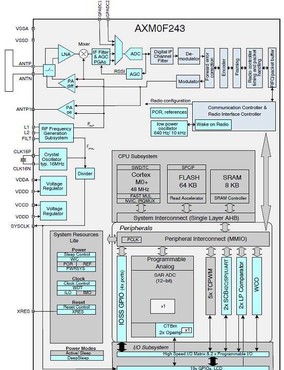
图1.AXM0F243框图
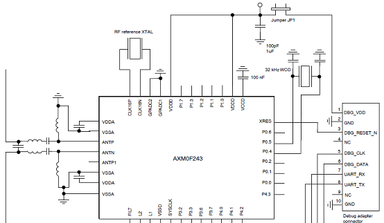
图2.AXM0F243典型应用框图:连接到调试适配器

图3.差分天线接口架构,TX/RX工作于50欧姆单端设备或天线

图4.单端天线接口架构,TX工作于50欧姆单端设备或天线

图5.单端天线接口架构,TX工作于50欧姆单端设备或天线
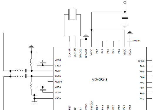
图6.采用双极天线和内部TX/RX开关的应用框图
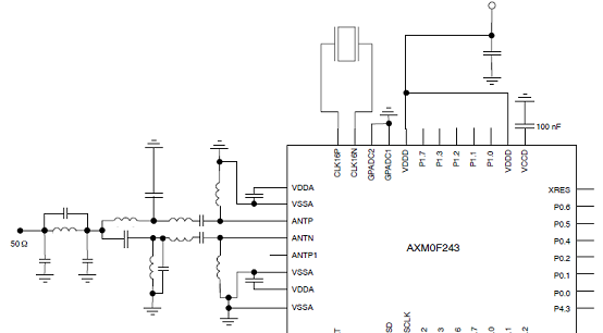
图7.采用单端天线和内部TX/RX开关的应用框图
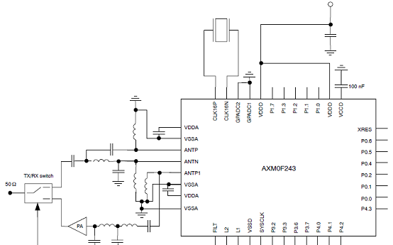
图8.采用单端天线和外接PA与天线开关的应用框图
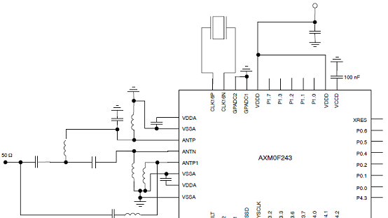
图9.采用单端天线和单端内部PA无RX/TX开关的应用框图
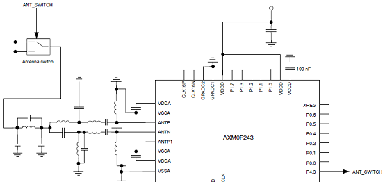
图10.采用两个单端天线和外接天线开关的应用框图

图11.采用外接VCO电感的应用框图
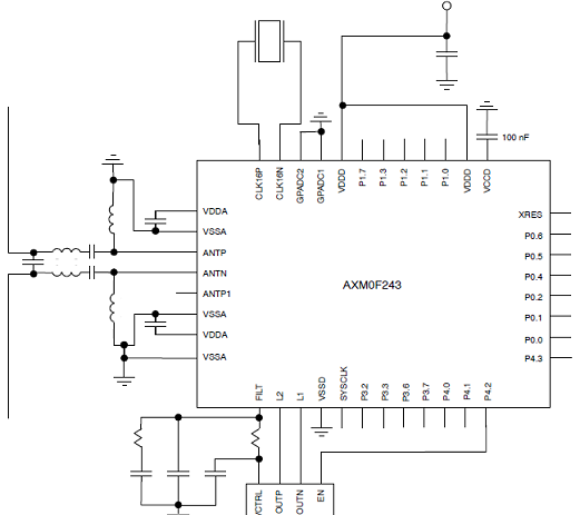
图12.采用外接VCO的应用框图

图13.采用TCXO的应用框图
评估板EVBUM2595/D
EVBUM2595/D DVK-AXM0F243-xxx-x-GEVK Evaluation Kit User ’s Manual
The DVK−AXM0F243−868−x−GEVK andDVK−AXM0F243−915−x−GEVK kits are designed as quick startsolution for the development of applications with the AXM0F243 RFSystem On Chip (SoC). This SoC combines an ARM Cortex M0+ultra−low power microcontroller with the AX5043 ultra−low powerRF transceiver in a single IC package. TheDVK−AXM0F243−868−x−GEVK is optimized for 868 MHzfrequency, and the DVK−AXM0F243−915−x−GEVK developmentkit is enhanced for 915 MHz. The DVK−AXM0F243−xxx−x−GEVK’s are compatible withAX−RadioLab and AxCode::Blocks development software for the PC.
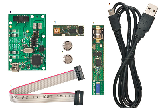
图14.评估板DVK−AXM0F243−868−x−GEVK套件外形图
The DVK−AXM0F243−868−x−SMA−GEVBmainboard isthe first of two boards in the DVK−AXM0F243−868−x−GEVKkit. It features the AXM0F243 ultra−low power SoC, as well asa LED, a button, and a 50 _ SMA port. In addition to theantennas shipped with the kit, various 50 _antennas withmale SMA connector can be used. The SMA port can also beused to connect the DVK to RF measurement equipment forconducted−mode testing. Similarly the DVK−AXM0F243−915−x−SMA−GEVBmainboard is the first of two boards in theDVK−AXM0F243−915−x−GEVK kit.
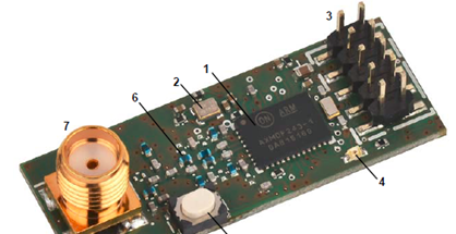
图14.DVK−AXM0F243−xxx−x−SMA−GEVB外形图
The DVK−AXM0F243−868−x−ANT−GEVB mainboard isthe second of two boards in the
DVK−AXM0F243−868−x−GEVK kit.
It features the AXM0F243 ultra−low power SoC, as wellas a LED, a button, battery, and chip antenna.Similarly the DVK−AXM0F243−915−x−ANT−GEVBmainboard is the first of two boards in theDVK−AXM0F243−915−x−GEVK kit.
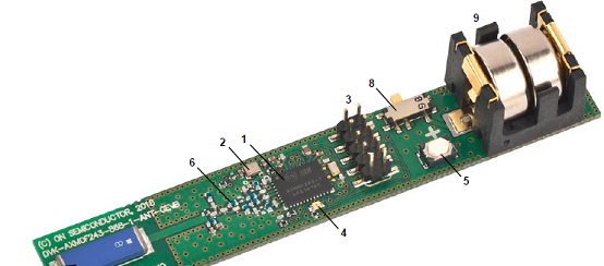
图15.DVK−AXM0F243−xxx−x−ANT−GEVB外形图
The AXDBG debug adapter is the interface between thePC and the mainboards. It can be used for programming anddebugging the AXM0F243 microcontroller. It interfaceswith the PC via windows drivers and the AXSDB softwareinterface, which is then used by AX−RadioLab andAxCode::Blocks development software for the PC. TheAXSDB can also be used in mass production with thescriptable AXSDB software.

图16.AXDBG调试适配器外形图
RF functionality are already programmed on bothmainboards. It’s possible to make the first RF experiencesending data packages fromDVK−AXM0F243−XXX−x−SMA−GEVB, programmedas transmitter, to theDVK−AXM0F243−XXX−x−ANT−GEVB, programmedas receiver, just following these simply steps.

图17.DVK-AXM0F243-xxx-x-SMA-GEVB连接图
责任编辑:David
【免责声明】
1、本文内容、数据、图表等来源于网络引用或其他公开资料,版权归属原作者、原发表出处。若版权所有方对本文的引用持有异议,请联系拍明芯城(marketing@iczoom.com),本方将及时处理。
2、本文的引用仅供读者交流学习使用,不涉及商业目的。
3、本文内容仅代表作者观点,拍明芯城不对内容的准确性、可靠性或完整性提供明示或暗示的保证。读者阅读本文后做出的决定或行为,是基于自主意愿和独立判断做出的,请读者明确相关结果。
4、如需转载本方拥有版权的文章,请联系拍明芯城(marketing@iczoom.com)注明“转载原因”。未经允许私自转载拍明芯城将保留追究其法律责任的权利。
拍明芯城拥有对此声明的最终解释权。


 产品分类
产品分类




 2012- 2022 拍明芯城ICZOOM.com 版权所有 客服热线:400-693-8369 (9:00-18:00)


