Microsemi双路SiC MOSFET参考设计MSCSICMDD/REF1
 69
69
 拍明
拍明
原标题:Microsemi双路SiC MOSFET参考设计MSCSICMDD/REF1
Microsemi公司的MSCSICMDD/REF1是双路SiC MOSFET驱动器参考设计,是开源解决方案,提供了用户友好的设计指南,使得用户采用MicrosemiSiC MOSFET能更快地走向市场.参考设计还支持过度到下代SiC MOSFET,新的参考设计为用户提供了高度绝缘的SiC MOSFET双栅极驱动器开关,用作评估各种拓扑中SiC MOSFET的方法.这包括有同步死区时间保护的半桥开关闭优化模式,以及没有保护的异步信号传输.它还配置成提供共流驱动以了解无阻尼感应开关(UIS)或双脉冲测试.参考设计仅需要24V电源输入,两个栅极驱动的隔离大于2000V,每边栅极驱动能力8W,栅极驱动电压–5 V/20 V,峰值输出电流高达±30 A,高达400kHz开关频率,单端或RS485/RS422差分输入栅极控制,±100 kV/μs功能,故障信令,可配置开关死区时间,非常低的时序抖动.主要用在航空航天(激励,空调,电源分配),汽车电子(混合/电动汽车动力总成,电动汽车电池充电器,DC/DC转换器和能量恢复),国防(电源,大功率马达驱动),工业(光伏逆变器,马达驱动,焊接机,UPS,开关电源,电感加热,石油钻井)以及医疗(MRI,X射线电源).本文介绍了SiCMSCSICMDD/REF1参考设计主要特性,框图和半桥框图,电路图和材料清单.
The dual SiC MOSFET driver reference design is an open-source solutionthat provides user-friendly design guides, enabling faster time-to-marketfor customers using MicrosemiSiC MOSFETs. The reference design alsosupports the transition to Microsemi’s next-generation SiC MOSFETs.
The new reference design provides customers with a highly isolated SiCMOSFET dual-gate driver switch as a means of evaluating SiC MOSFETsin a number of topologies. This includes modes optimized for half-bridgeswitching with synchronous dead-time protection and asynchronoussignal transfer with no protection. It can also be configured to provideconcurrent drive to study unclamped inductive switching (UIS) or doublepulse testing. The board supports the modification of gate resistor values toaccommodate most Microsemidiscretes and modules.
The dual SiC MOSFET driver reference design is ideal for a wide rangeof end markets and applications, including aerospace (actuation, airconditioning, and power distribution), automotive (hybrid/electric vehiclepowertrains), electric vehicle battery chargers, DC-to-DC converters, andenergy recovery), defense (power supply and high-power motor drive),industrial (photovoltaic inverters, motor drives), welding, uninterruptiblepower supply, switched-mode power supply, induction heating, and oildrilling), and medical (MRI and X-ray power supply).
SiCMSCSICMDD/REF1参考设计主要特性:
• Switch configurable as either a high/low sidedriver with half bridges or independent drive
• Requires only a 24 V power input
• Galvanic isolation of more than 2000 V on bothgate drivers
• Capable of 8 W of gate drive power per side
• Peak output current of up to ±30 A
• Up to 400 kHz maximum switching frequency
• Single-ended or RS485/RS422 differential inputgate control
• Desaturation shoot-through (short-circuit)protection
• ±100 kV/μs capability
• Fault signaling
• SiC compatible under voltage lockoutprotection
• Gate drive voltage is –5 V/20 V and adjustablefor lower voltages
• Switch-configurable dead time
• Option of disabling shoot-through protection fordual switch UIS/RUIS testing
• Very low timing skew
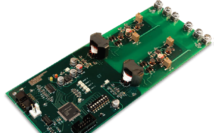
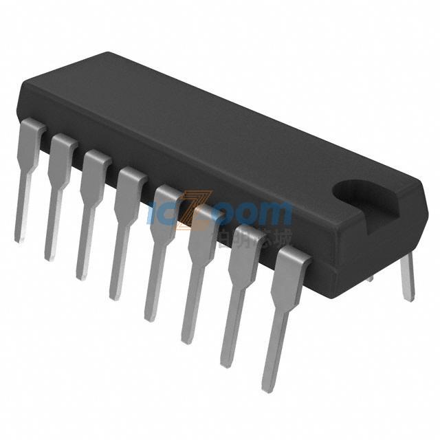
图1.双路SiC MOSFET参考设计MSCSICMDD/REF1外形图
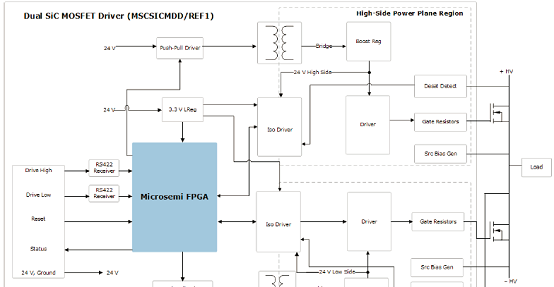
图2.双路SiC MOSFET驱动器参考设计MSCSICMDD/REF1框图
The dual SiC MOSFET driver reference design (MSCSICMDD/REF1) includes an evaluation board
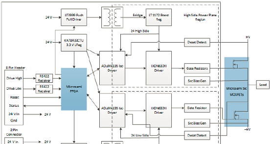
图3.半桥框图
The reference design is optimized to drive SiC MOSFET devices at high-speeds with desaturationprotection. It is a base design that can be simplified depending upon the individual systemrequirements.
参考设计MSCSICMDD/REF1主要特性:
Requires only a 24 V power input
Adjustable –5 V, +20 V output gate drive
Galvanic isolation of more than 2000 V on both gate drivers
Capable of 6 W of gate-drive power/side (8 W with modification)
Peak output current up to 30 A
Maximum switching frequency greater than 400 kHz
Single-ended or RS485/RS422 differential input gate control
Shot-through (short-circuit) protection
±100 kV/μs capability
Programmable dead time protection
Fault signaling
Under voltage lockout protection
Note: The board has been tested to 400 kHz.Any calculation of gate-power drive must include thefrequency dependent portion of the driver IXDN630 and the ADuM4135.
This design uses an analog device (ADuM4135) to pass signals across the isolation boundary. The deviceis a good fit for the application, with the exception that the under voltage lockout on the gate side isnominally 11 V, which is rather low for SiC MOSFETs. The ADuM4135 has a 4 A driver. To work aroundthe low UVLO and to increase the output current, the output is buffered through an IXDN630 driver. Azener diode is added in the positive leg of the ADuM4135 to increase the UVLO trip point toapproximately 18 V.
With any gate driver, there is a need to transfer energy across the isolation interface to drive the gates.
Most standard isolation supplies are not designed with adequate insulation, a low-capacitance interface,or tolerance to the high dV/dt associated with SiC MOSFETs in a half bridge. Consider that 10 pF ofcapacitance across the barrier translates to a 350 mA current spike back into the gate supply and itsassociated grounding. It is desirable to keep the capacitance across the gate supply transformer to aminimum.
Power is transferred across the isolation boundary with an LTC3999 switching IC followed by a customtransformer. Power is transferred unregulated over the boundary and then regulated on the gate side.
This decouples the isolation transformer design from the regulator design.
Microsemi’s FPGA controls power sequencing. In the first 0.5 second, the FPGA reduces the poweravailable from the LTC3999. During this time, switching is blocked, hence there will be little demand forpower and the LTC3999 can only deliver about 1 W. After the timeout, if there is no fault condition,power capability is increased to approximately 6 W. If at any time a fault is flagged by one of theADuM4135s, then switching is cut off to both drivers and power is reduced. This protects the LTC3999against a shorted load as this board is used for product development and generally should surviveoutput device failures.
The gate power transformer is constructed from an RM8 core by Fair-rite, part number 6278230121, abobbin by Loadstone, part number B-RM8-2-PH. The wire is by Belden, part number 8053 doubleinsulated magnet wire. The primary is 26 turns center tapped, 26 Gauge. The secondary is 13 turns, 26Gauge. The core is electrically conductive so some of the pins closer to the core have been removed toincrease clearance. The split bobbin design results in a primary-to-secondary capacitance of only a fewpicofarads and provides good electrical isolation.
参考设计MSCSICMDD/REF1目标应用:
Aerospace (actuation, air conditioning, power distribution)
Automotive (hybrid/electric vehicle powertrains, electric vehicle battery chargers, DC-to-DC converters, energy recovery)
Defense (power supply, high power motor drive)
Industrial (photovoltaic inverters, motor drives, welding, uninterruptible power supply, switched-mode power supply, induction heating, oil drilling)
Medical (MRI, X-ray power supply)
连接器" src="https://supp.iczoom.com/images/public/201910/1570771910870065852.png" width="463" height="151" border="0" vspace="0" title="连接器" style="width: 463px; height: 151px;"/>
图4.连接器
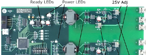
图5.LED和测试点
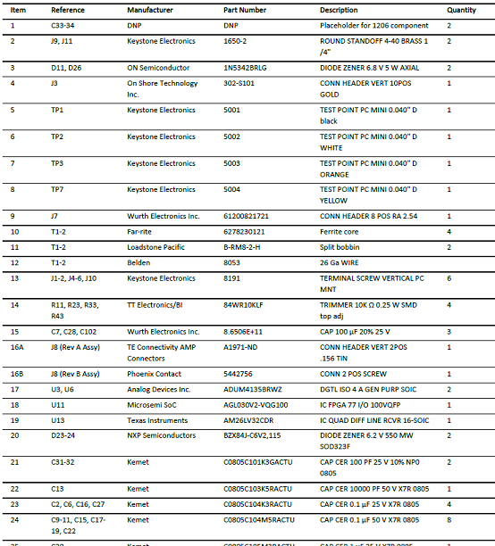
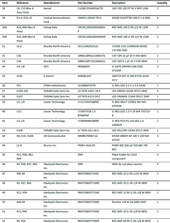
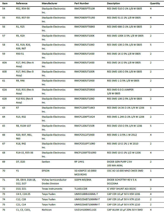
参考设计MSCSICMDD/REF1材料清单:
责任编辑:David
【免责声明】
1、本文内容、数据、图表等来源于网络引用或其他公开资料,版权归属原作者、原发表出处。若版权所有方对本文的引用持有异议,请联系拍明芯城(marketing@iczoom.com),本方将及时处理。
2、本文的引用仅供读者交流学习使用,不涉及商业目的。
3、本文内容仅代表作者观点,拍明芯城不对内容的准确性、可靠性或完整性提供明示或暗示的保证。读者阅读本文后做出的决定或行为,是基于自主意愿和独立判断做出的,请读者明确相关结果。
4、如需转载本方拥有版权的文章,请联系拍明芯城(marketing@iczoom.com)注明“转载原因”。未经允许私自转载拍明芯城将保留追究其法律责任的权利。
拍明芯城拥有对此声明的最终解释权。


 产品分类
产品分类




 2012- 2022 拍明芯城ICZOOM.com 版权所有 客服热线:400-693-8369 (9:00-18:00)


