


 产品分类
产品分类
基于Linear LTC2185双路16位125Msps模数转换方案
 88
88
 拍明
拍明
原标题:Linear LTC2185双路16位125Msps模数转换方案
Linear 公司的LTC2185是双路16位125Msps低功耗模数转换器(ADC), 两路可同时取样, 76.8dB SNR, 90dB SFDR,单电源1.8V工作,每路功耗185mW/154mW/100mW, CMOS, DDR CMOS或DDR LVDS输出,输入范围1VP-P到 2VP-P,550MHz满功率带宽S/H,主要用在通信, 蜂窝基站,SDR,手提医疗图像,多路数据采集以及非破坏测试.本文介绍了LTC2185主要特性, 方框图,多种模拟输入和前端电路,以及典型应用电路和PCB布局图.
LTC2185 - 16-Bit, 125Msps Low Power Dual ADCs
The LTC.2185/LTC2184/LTC2183 are two-channel simultaneous sampling 16-bit A/D converters designed for digitizing high frequency, wide dynamic range signals.
They are perfect for demanding communications applications with AC performance that includes 76.8dB SNR and 90dB spurious free dynamic range (SFDR). Ultralow jitter of 0.07psRMS allows undersampling of IF frequencies with excellent noise performance. DC specs include ±2LSB INL (typ), ±0.5LSB DNL (typ) and no missing codes over temperature. The transition noise is 3.4LSBRMS.
The digital outputs can be either full rate CMOS, Double Data Rate CMOS, or Double Data Rate LVDS. A separate output power supply allows the CMOS output swing to range from 1.2V to 1.8V.
The ENC+ and ENC– inputs may be driven differentially or single-ended with a sine wave, PECL, LVDS, TTL, or CMOS inputs. An optional clock duty cycle stabilizer allows high performance at full speed for a wide range of clock duty cycles.
LTC2185主要特性:
Two-Channel Simultaneously Sampling ADC
76.8dB SNR
90dB SFDR
Low Power: 370mW/308mW/200mW Total
185mW/154mW/100mW per Channel
Single 1.8V Supply
CMOS, DDR CMOS, or DDR LVDS Outputs
Selectable Input Ranges: 1VP-P to 2VP-P
550MHz Full Power Bandwidth S/H
Optional Data Output Randomizer
Optional Clock Duty Cycle Stabilizer
Shutdown and Nap Modes
Serial SPI Port for Configuration
64-Pin (9mm × 9mm) QFN Package
LTC2185应用:
Communications
Cellular Base Stations
Software Defined Radios
Portable Medical Imaging
Multi-Channel Data Acquisition
Nondestructive Testing

图1.LTC2185方框图
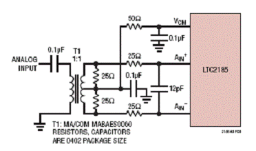
图2.LTC2185采用变压器5MHz-700MHz模拟输入电路图

图3.LTC2185输入频率5MHz-150MHz的前端电路图
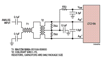
图4.LTC2185输入频率150MHz-250MHz的前端电路图
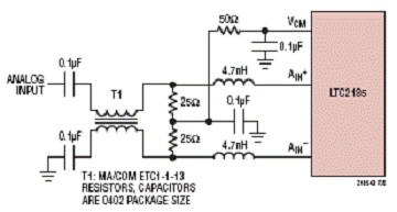
图5.LTC2185输入频率大于250MHz的前端电路图
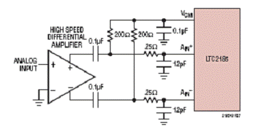
图6.LTC2185采用高速差分放大器的前端电路图
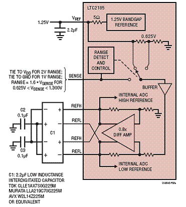
图7.LTC2185基准电路图
责任编辑:HanFeng
【免责声明】
1、本文内容、数据、图表等来源于网络引用或其他公开资料,版权归属原作者、原发表出处。若版权所有方对本文的引用持有异议,请联系拍明芯城(marketing@iczoom.com),本方将及时处理。
2、本文的引用仅供读者交流学习使用,不涉及商业目的。
3、本文内容仅代表作者观点,拍明芯城不对内容的准确性、可靠性或完整性提供明示或暗示的保证。读者阅读本文后做出的决定或行为,是基于自主意愿和独立判断做出的,请读者明确相关结果。
4、如需转载本方拥有版权的文章,请联系拍明芯城(marketing@iczoom.com)注明“转载原因”。未经允许私自转载拍明芯城将保留追究其法律责任的权利。
拍明芯城拥有对此声明的最终解释权。
相关资讯
:
基于MC33771主控芯片的新能源锂电池管理系统解决方案

AMIC110 32位Sitara ARM MCU开发方案

基于AMIC110多协议可编程工业通信处理器的32位Sitara ARM MCU开发方案

基于展讯SC9820超低成本LTE芯片平台的儿童智能手表解决方案

基于TI公司的AM437x双照相机参考设计

基于MTK6580芯片的W2智能手表解决方案


 2012- 2022 拍明芯城ICZOOM.com 版权所有 客服热线:400-693-8369 (9:00-18:00)


