


 产品分类
产品分类
Renesas RX630系列32位MCU开发方案
 77
77
 拍明
拍明
原标题:Renesas RX630系列32位MCU开发方案
Renesas公司的RX630系列是32位mcu,工作频率最大为100MHz,100MHz时的性能为165 DMIPS,具有单精度32位IEEE-754浮点,两种类型的乘法和累加器,工作电压2.7V-3.6V,主要用在嵌入式系统.本文介绍了RX630系列主要特性,方框图,RX630系列评估板主要特性与指标,方框图,电路图和元件布局图.
RX630系列主要特性:
■ 32-bit RX CPU core
Max. operating frequency: 100 MHz
Capable of 165 DMIPS in operation at 100 MHz
Single precision 32-bit IEEE-754 floating point
Two types of multiply-and-accumulation unit (between memories and between registers)
32-bit multiplier (fastest instruction execution takes one CPU clock cycle)
Divider (fastest instruction execution takes two CPU clock cycles)
Fast interrupt
CISC Harvard architecture with 5-stage pipeline
Variable-length instructions: Ultra-compact code
Supports the memory protection unit (MPU)
JTAG and FINE (two-line) debugging interfaces
■ Low-power design and architecture
Operation from a single 2.7- to 3.6-V supply
Low power consumption: A product that supports all peripheral functions draws only 500 μA/MHz.
RTC is capable of operation from a dedicated power supply (min. operating voltage: 2.3 V).
Four low-power modes
■ On-chip main flash memory, no wait states
100-MHz operation, 10-ns read cycle (no wait states)
384-Kbyte to 2-Mbyte capacities
User code programmable via the USB, SCI, or JTAG
■ On-chip data flash memory
Max. 32 Kbytes, reprogrammable up to 100,000 times
Programming/erasing as background operations (BGOs)
■ On-chip SRAM, no wait states
32- to 128-Kbyte capacities
For instructions and operands
Can provide backup on deep software standby
■ DMA
DMAC: Incorporates four channels
DTC
■ Reset and supply management
Power-on reset (POR)
Low voltage detection (LVD) with voltage settings
■ Clock functions
External crystal oscillator or internal PLL for operation at 4 to 16 MHz
Internal 125-kHz LOCO and 50-MHz HOCO
Dedicated 125-kHz LOCO for the IWDT
Frequency of the oscillator for sub-clock generation: 32 kHz
■ Real-time clock
Adjustment functions (30 seconds, leap year, and error)
Time capture function (for capturing times in response to event-signal input on external pins)
■ Independent watchdog timer
125-kHz LOCO clock operation
■ Useful functions for IEC60730 compliance
Oscillation-stop detection, frequency measurement, CRC, IWDT, self-diagnostic function for the A/D converter, etc.
■ Up to 22 communications interfaces
USB 2.0 full-speed function interface (1 channel)
CAN (compliant with ISO11898-1), incorporating 32 mailboxes (up to 3 channels)
SCI with multiple functionalities (up to 13 channels)
Choose from among asynchronous mode, clock-synchronous mode, smart-card interface mode, simple SPI, simple I2C, and extended serial mode.
I2C bus interface for transfer at up to 1 Mbps (up to 4 channels)
RSPI for high-speed transfer (up to 3 channels)
■ External address space
8 CS areas (8 × 16 Mbytes)
Multiplexed address data or separate address lines are selectable per area.
8-, 16-, or 32-bit bus space is selectable per area
■ Up to 20 extended-function timers
16-bit MTU2: input capture, output capture, complementary PWM output, phase-counting mode (6 channels)
16-bit TPU: input capture, output capture, phase-counting mode (12 channels)
8-bit TMR (4 channels)
16-bit compare-match timers (4 channels)
■ A/D converter for 1-MHz Operation
Up to 21 12-bit channels, and incorporating 1 sample-and-hold circuit
Up to 8 10-bit channels, and incorporating 1 sample-and-hold circuit
Addition of results of A/D conversion (in the 12-bit A/D converter)
Self diagnosis (for the 10-bit A/D converter)
■ 10-bit D/A converter: 2 channels
■ Temperature sensor for measuring temperature within the chip
■ Register write protection function can protect values in important registers against overwriting.
■ Up to 148 pins for GPIO
5-V tolerance, open drain, input pull-up, switchable driving ability
■ Operating temp. range
–40 degree C to +85 degree C

图1.RX630系列方框图
RX630系列评估板
The Renesas Starter Kit for RX630 is intended as a user-friendly introductory and evaluation tool for the RX630 microcontroller. The kit also provides a useful platform for evaluating the Renesas suite of development tools for coding and debugging. This includes a choice of IDEs between the High-performance Embedded Workshop and e2studio.
The Renesas Starter Kit for RX630 may be connected to the host PC using a simple RS232 serial connection or via the included USB E1 on chip debugging interface.
The purpose of the board is to enable the user to evaluate the capabilities of the device and its peripherals by giving the user a simple platform on which code can be run only minutes from opening box. It can also prove an invaluable tool in development by providing a useful test platform for code already debugged using one of our more powerful emulation tools.
This RSK is an evaluation tool for Renesas microcontrollers. This manual describes the technical details of the RSK hardware. The Quick Start Guide and Tutorial Manual provide details of the software installation and debugging environment.
RX630系列评估板主要特性:
This RSK provides an evaluation of the following features:
Renesas microcontroller programming
User code debugging
User circuitry such as switches, LEDs and a potentiometer
Sample application
Sample peripheral device initialisation code
The RSK board contains all the circuitry required for microcontroller operation.

图2.RX630系列评估板方框图
The LCD display module is supplied as a detachable sub-board. The board dimensions are 120 mm by 100 mm, detailed dimensions are available in the user manual.
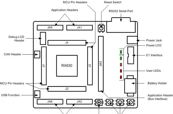
图3.RX630系列评估板元件布局图
RX630系列评估板主要指标:
Item | Specification |
Microcontroller | R5F5630EDDFP |
Input Clock | Main: 12 MHz |
Sub: 32.768 kHz | |
Potentiometer | Single-turn, 10 kΩ |
LED | Power indicator: green x 1 |
User: green x 1, orange x 1, red x 2 | |
Switch | Reset x 1 |
User x 3 | |
DC Power Jack | 5 V Input |
Battery Holder | CR2032 |
E1 Header | 14-pin box header |
CAN Connector | 2.54 mm pitch, 3-pin (CAN BUS line x 2, GND x 1) |
USB Connector | Function: USB-MiniB |
RS232 Serial Connector | 9-pin DSUB |
LCD Display Connector | 14-pin socket |
Microcontroller Pin Header | 2.54 mm pitch, 36-pin x 4 (J1, J2, J3, J4) |
Application Board Interface | 2.54 mm pitch, 26-pin x 2 (JA1, JA2), 24-pin x 2 (JA5, JA6) |
BUS Interface Option | 2.54 mm pitch, 50-pin (JA3) |

图4.RX630系列评估板外形图
责任编辑:HanFeng
【免责声明】
1、本文内容、数据、图表等来源于网络引用或其他公开资料,版权归属原作者、原发表出处。若版权所有方对本文的引用持有异议,请联系拍明芯城(marketing@iczoom.com),本方将及时处理。
2、本文的引用仅供读者交流学习使用,不涉及商业目的。
3、本文内容仅代表作者观点,拍明芯城不对内容的准确性、可靠性或完整性提供明示或暗示的保证。读者阅读本文后做出的决定或行为,是基于自主意愿和独立判断做出的,请读者明确相关结果。
4、如需转载本方拥有版权的文章,请联系拍明芯城(marketing@iczoom.com)注明“转载原因”。未经允许私自转载拍明芯城将保留追究其法律责任的权利。
拍明芯城拥有对此声明的最终解释权。
相关资讯
:
基于MC33771主控芯片的新能源锂电池管理系统解决方案

AMIC110 32位Sitara ARM MCU开发方案

基于AMIC110多协议可编程工业通信处理器的32位Sitara ARM MCU开发方案

基于展讯SC9820超低成本LTE芯片平台的儿童智能手表解决方案

基于TI公司的AM437x双照相机参考设计

基于MTK6580芯片的W2智能手表解决方案


 2012- 2022 拍明芯城ICZOOM.com 版权所有 客服热线:400-693-8369 (9:00-18:00)


