Renesas RX63N 32位RX MCU开发方案
 75
75
 拍明
拍明
原标题:Renesas RX63N 32位RX MCU开发方案
Renesas公司的RX63N是100MHz 32位RX mcu ,165DMIPS性能,集成了多达2MB闪存,以太网MAC,全速USB 2.0主/功能/OTG接口,包括CAN的各种通信接口,10位和12位ADC和RTC.和现有产品相比,待机功耗降低大约90%,工作电压2.7- 3.6V,主要用在音频设备,马达控制,游戏机和通信设备.本文介绍了RX63N主要特性,方框图,RX63N开发套件应用和特性,方框图,电路图和材料清单.
The RX63N/RX631 Group incorporates communication functions suitable for networking equipment, such as Ethernet controller, USB 2.0 full-speed (function, host, or OTG selectable), and CAN. In addition, with a RTC (Real-Time Clock) that can operate on a dedicated power supply as a low power feature, standby power consumption can be reduced by approximately 90% compared to existing products. The selection of on-chip memory has been expanded from ROMless to 2 MB, and even smaller-sized packages are available. This makes possible mounting in anything from large-scale systems to small-scale/small-space devices.
RX63N主要特性:
32-bit RX CPU core
Max. operating frequency: 100 MHz
Capable of 165 DMIPS in operation at 100 MHz
Single precision 32-bit IEEE-754 floating point
Two types of multiply-and-accumulation unit (between memories and between registers)
32-bit multiplier (fastest instruction execution takes one CPU clock cycle)
Divider (fastest instruction execution takes two CPU clock cycles)
Fast interrupt
CISC Harvard architecture with 5-stage pipeline
Variable-length instructions: Ultra-compact code
Supports the memory protection unit (MPU)
JTAG and FINE (two-line) debugging interfaces
Low-power design and architecture
Operation from a single 2.7- to 3.6-V supply
Low power consumption: A product that supports all peripheral functions draws only 500uA/MHz.
RTC is capable of operation from a dedicated power supply (min. Operating voltage: 2 V).
Four low-power modes
On-chip main flash memory, no wait states
Supports ROM-less versions and versions with up to 2 Mbytes of ROM (ROM-less version: RX631 Group only)
100-MHz operation, 10-ns read cycle (no wait states)
384-Kbyte to 2-Mbyte capacities
User code programmable via the USB, SCI, or JTAG
On-chip data flash memory
ROM-less or 32 Kbytes of ROM (reprogrammable up to 100,000 times)
Programming/erasing as background operations (BGOs)
On-chip SRAM, no wait states
32- to 128-Kbyte capacities
For instructions and operands
Can provide backup on deep software standby
DMA
DMAC: Four channels
DTC
EXDMAC: Two channels
Dedicated DMAC for the Ethernet controller: Single channel
Reset and supply management
Power-on reset (POR)
Low voltage detection (LVD) with voltage settings
Clock functions
External crystal oscillator or internal PLL for operation at 4 to 16 MHz
Internal 125-kHz LOCO and 50-MHz HOCO
Dedicated 125-kHz LOCO for the IWDT
Real-time clock
Adjustment functions (30 seconds, leap year, and error)
Time capture function (for capturing times in response to event-signal input on external pins)
Independent watchdog timer
125-kHz LOCO clock operation
Useful functions for IEC60730 compliance
Oscillation-stoppage detection, frequency measurement, CRC, IWDT, selfdiagnostic function for the A/D converter, etc.
Various communications interfaces
Ethernet MAC (1) (not in RX631 Group products)
Host/function or OTG controller (1) and function controller (1) with fullspeed USB 2.0 transfer
CAN (compliant with ISO11898-1), incorporating 32 mailboxes (up to 3 modules)
SCI with multiple functionalities (up to 13)
Choose from among asynchronous mode, clock-synchronous mode, smartcard interface mode, simplified SPI, simplified I2C, and extended serial mode.
I2C bus interface for transfer at up to 1 Mbps (up to 4)
RSPI for high-speed transfer (up to 3)
External address space
Buses for high-speed data transfer (max. operating frequency of 50 MHz)
8 CS areas (8 ⊙ 16 Mbytes)
Multiplexed address data or separate address lines are selectable per area.
8-, 16-, or 32-bit bus space is selectable per area
Independent SDRAM area (128 Mbytes)
Up to 20 extended-function timers
16-bit MTU2: input capture, output compare, PWM waveform output, phase-counting mode (6 channels)
16-bit TPU: input capture, output compare, phase-counting mode (12 channels)
8-bit TMR (4 channels)
16-bit compare-match timers (4 channels)
A/D converter for 1-MHz Operation
Up to 21 12-bit channels, and incorporating 1 sample-and-hold circuit
Up to 8 10-bit channels, and incorporating 1 sample-and-hold circuit
Addition of results of A/D conversion (in the 12-bit converter)
Self diagnosis (for the 10-bit converter)
10-bit D/A converter: 2 channels
Temperature sensor for measuring temperature within the chip
Register write protection can protect values in important registers against overwriting.
Up to 134 pins for GPIO
5-V tolerance, open drain, input pull-up, switchable driving ability
Operating temp. range -40 degree C to +85 degree C

图1。RX63N方框图
RX63N开发套件
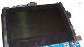
Renesas Demonstration Kit (RDK) for RX63N
This RDK is an evaluation and demonstration tool for Renesas RX63N microcontrollers. The goal is to provide the user with a powerful debug and demonstration platform targeted at common applications. A set of human/machine interfaces are tightly integrated with the features of the RX63N and the software demonstration programs providing the user with an accessible platform to rapidly evaluate and customize.
RX63N开发套件应用和特性:
• Audioo
Stereo audio driver connected to the PWM interface
On-board microphone to demonstrate sampling, FFT/FPU capabilities
Volume Control Potentiometer
Micro SD card interface for audio and data files
• Motor Control
3 –Phase motor control algorithm representation with LEDs
Motor control algorithm speed variation through volume control potentiometer
• Gaming
3 –Axis Accelerometer (Digital)
User pushbutton switches
• Communications
10/100 Ethernet Interface connected to an internal Ethernet MAC (1588 compatible)
USB Interface connected to an internal USB controller (Host, Device and OTG)
RS-232 Interface
CAN Interface
I2C, SPI with Debug through the Beagle connector from Total Phase
PMOD connections to support a variety of generic PMOD devices (WiFi, Bluetooth, RF, and much more).
• User Code and Application Debugging
On-board J-Link OB for high-quality source code debugging

图2。RX63N开发套件外形图

图3。RX63N开发套件方框图
责任编辑:HanFeng
【免责声明】
1、本文内容、数据、图表等来源于网络引用或其他公开资料,版权归属原作者、原发表出处。若版权所有方对本文的引用持有异议,请联系拍明芯城(marketing@iczoom.com),本方将及时处理。
2、本文的引用仅供读者交流学习使用,不涉及商业目的。
3、本文内容仅代表作者观点,拍明芯城不对内容的准确性、可靠性或完整性提供明示或暗示的保证。读者阅读本文后做出的决定或行为,是基于自主意愿和独立判断做出的,请读者明确相关结果。
4、如需转载本方拥有版权的文章,请联系拍明芯城(marketing@iczoom.com)注明“转载原因”。未经允许私自转载拍明芯城将保留追究其法律责任的权利。
拍明芯城拥有对此声明的最终解释权。


 产品分类
产品分类




 2012- 2022 拍明芯城ICZOOM.com 版权所有 客服热线:400-693-8369 (9:00-18:00)


