


 产品分类
产品分类
Freescale Kinetis KW0x无线MCU开发方案
 191
191
 拍明
拍明
原标题:Freescale Kinetis KW0x无线MCU开发方案
freescale公司的Kinetis KW0x系列产品是低于1GHz的无线MCU,集成了支持FSK, GFSK, MSK或OOK调制的收发器和低功耗ARM® Cortex M0+ CPU.集成的收发器工作频率包括ISM频段的315 MHz, 433 MHz, 470 MHz, 868 MHz, 915 MHz, 928 MHz和955 MHz,主要用在自动读表,无线传感器网络,家庭和建筑物自动化,工业监控以及无线告警和安全系统.本文介绍了KW0x系列主要特性,框图和应用电路, MKW01收发器框图以及参考板MRB-KW0x和TWR-RF Module主要特性,电路图,多个频段的材料清单和PCB元件布局图.
The MKW01 device is highly-integrated, cost-effective, smart radio, sub-1 GHz wireless node solution composed of a transceiver supporting FSK, GFSK, MSK, or OOK modulations with a low-power ARM® Cortex M0+ CPU. The highly integrated RF transceiver operates over a wide frequency range including 315 MHz, 433 MHz, 470 MHz, 868 MHz, 915 MHz, 928 MHz, and 955 MHz in the license-free Industrial, Scientific and Medical (ISM) frequency bands. This configuration allows users to minimize the use of external components.
The MKW01 is targeted for the following low-power wireless applications:
• Automated Meter Reading
• Wireless Sensor Networks
• Home and Building Automation
• Wireless Alarm and Security Systems
• Industrial Monitoring and Control
Freescale supplements the MKW01 with tools and software that include hardware evaluation and development boards, software development IDE and applications, drivers, custom PHY usable with Freescale’s IEEE 802.15.4 compatible MAC and SMAC.
KW0x系列主要特性:
• RF Transceiver Features
— Operating Voltage from 1.8V to 3.6V.
— Programmable bit rate up to 600kbps (FSK)
— High Sensitivity: down to -120 dBm at 1.2 kbps
— High Selectivity: 16-tap FIR Channel Filter
— Bullet-proof front end: IIP3 = -18 dBm, IIP2 = +35 dBm, 80 dB Blocking Immunity, no Image
Frequency response
— Low current: Rx = 16mA, 100nA register retention
— Programmable Pout : -18 to +17 dBm in 1 dB steps
— Constant RF performance over voltage range of chip
— Fully integrated synthesizer with a resolution of 61 Hz
— FSK, GFSK, MSK, GMSK and OOK modulations
— Built-in Bit Synchronizer performing Clock recovery
— Incoming Sync Word Recognition
— Automatic RF Sense with ultra-fast AFC
— Packet engine with CRC, AES-128 encryption and 66-byte FIFO
— Built-in temperature sensor and Low battery indicator
— 32 MHz crystal oscillator clock source
— Dedicated I/O’s for connection with an external 32 kHz crystal
• MCU Features
System:
— 48 MHz Max. Central Processor Unit (CPU) frequency
— 24 MHz Max. Bus frequency
— Vectored Interrupt Controller (NVIC) with 32 core-vectored interrupts with 4 programmable
interrupt priority levels
— Asynchronous Wake-up Interrupt Controller (AWIC)
— 4 channel Direct Memory Access (DMA)
— DMA request multiplex
— Non Maskable Interrupt (NMI)
— COP Watchdog
— Low leakage Wake-up Unit (LLWU)
— Debug and Trace
– 2-pin Serial Wire Debug (SWD)
—80-bit wide ID number
Memory:
— 128 KB P-Flash with 64 byte flash cache
— 16 KB RAM
Clocks:
— External crystal oscillator or resonator:
– 32 - 40 kHz low range, low power or full swing
– 3 MHz - 32 MHz high range, low power or full swing
— DC - 48 MHz external square wave input clock
— Internal clock references:
– 31.25 kHz to 39.063 kHz oscillator with +/– 1.5% max. deviation from 0 to +70C
– 4 MHz oscillator with +/– 3% max. deviation across temperature
– 1 kHz oscillator
— Phase Locked Loop (PLL) with up to 100 MHz VCO
— Frequency Locked Loop (FLL):
– Low range: 20 - 25 MHz
– Mid range: 40 - 48 MHz
Analog:
— Power Management Controller (PMC) with low voltage warning (LVW) and detect with
selectable trip points.
— 16-bit analog to digital converter
– 11 single ended channels available
– 2 status, control and results registers
– DMA support
— 1 High Speed Comparator (HSCMP) with internal 6-bit digital to analog converters (DAC)
— One 12-bit DAC with DMA support and 2 word data buffer
Timers:
— Six channel Timer/PWM (TPM)
— Periodic interrupt timers
— 16-bit low-power timer (LPTMR) can be configured to operate as a time counter or as a pulse
counter, across all power modes, including the low-leakage modes
— Real-time clock 32-bit timer
Wired Communication Interface:
— One Serial Peripheral Interface (SPI) available externally
— Two Inter-Integrated Circuits (I2C) with DMA support
— Three Universal Asynchronous Receiver / Transmitter (UART) with DMA Support
– UART0 supports standard features plus:
• TxD pin can be configured as pseudo open drain for 1-wire half-duplex
• x4 to x32 oversampling
• Functional in VLPS mode
• LIN slave operation
– UART1 and UART2 support standard features
Human Machine Interface (HMI)
— General Purpose Input/Output (GPIO) supporting:
– Default to disabled (no leakage)
– 4 pins with 18 mA high current drive capability
– Hysteresis and configurable pull up device on all input pins
– Slew rate and drive strength fixed on all output pins
– Single cycle GPIO control via IOPORT
— Touch Sensor Inputs (TSI)
– 9-channel
– Selectable single channel wakeup source available in all modes
– DMA support
— Pin Interrupt
1.8 V to 3.6 V operating voltage with on-chip voltage regulators
Temperature range of –40C to 85C
60-pin LGA (8x8 mm) package
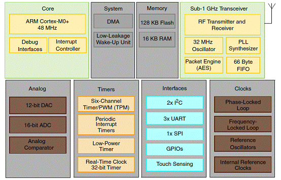
图1. KW0x系列框图

图2. MKW01收发器框图
Kinetis KW0x系列MCU模块参考板MRB-KW0x
MRB-KW0x: Modular Reference Boards for Kinetis KW0x Family of MCUs
The MKW01development platform is an evaluation environment based on the Freescale MKW01Z128CHN device. The MKW01Z128CHN is a highly-integrated, cost-effective, system-in-package (SIP), sub-1GHz wireless node solution with an FSK, GFSK, MSK, or OOK modulation-capable transceiver and low-power ARM Cortex M0+CPU microcontroller. The highly integrated RF transceiver operates over a wide frequency range including 315 MHz, 433 MHz, 470 MHz,868 MHz, 915 MHz, 928 MHz, and 955 MHz in the license-free Industrial, Scientific and Medical (ISM) frequency bands. This configuration allows users to minimize the use of external components.
The MKW01Z128CHN is targeted for the following low-power wireless applications:
• Automated Meter Reading
• Wireless Sensor Networks
• Home and Building Automation
• Wireless Alarm and Security Systems
• Industrial Monitoring and Control
• Wireless MBUS Standard (EN13757-4:2005)
Freescale supplements the MKW01Z128CHN with tools and software that include hardware evaluation and development boards, software development IDE and applications, drivers, custom PHY usable with Freescale’s IEEE 802.15.4 compatible MAC, and an available wireless MBUS solution.
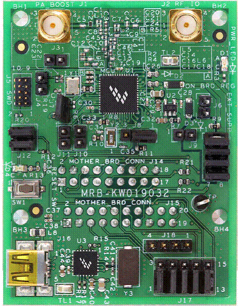
图4.参考板MRB-KW01外形图
MRB-KW01开发平台主要特性:
• Based on Freescale’s low-cost MKW01Z128CHN sub-1GHz wireless node solution with an FSK,GFSK, MSK, or OOK modulation-capable transceiver and low-power ARM Cortex M0+CPU microcontroller, and a functional set of MCU peripherals into a 60-pin LGA package
• Reference design area with small footprint, low cost RF node
— Power Amplifier Output
— Unbalanced input/output port
— Flexible RF-Front End for different bands operation
— Programmable output power from -18 dBm to +17 dBm in 1dB steps
— High Sensitivity: down to -120dBm at 1.2kbps
• 30 or 32 MHz reference oscillator depending on regional configuration
• SWD MCU debug port
• Optional secondary 32.768 kHz crystal for accurate low power RTC timing
• Master reset switch
• Full power regulation and management
• KW01-MRB board provides
— Required circuitry for MKW01Z128CHN - crystals and RF circuitry including SMA connectors for Power Amplifier Output and Input/Output RF port
— Local power supply regulation
— Access to all GPIO
— Standalone or daughter card use modes
— SWD connector
— Onboard UART communication via mini-USB connector.
— Two boards allow board-to-board packet communications
TWR-RF Module主要特性:
The KW01-MRB can run in the Freescale Tower System using the RF-Tower module (TWR-RF). Features of the TWR-RF module include:
• Standard sockets 100 mils J5 and J4 (2 x 9 and 2 x 10) to connect either a 1323x Modular Reference Board (1323x-MRB), a 12311 Modular Reference Board (12311-MRB) or a KW01 Modular Reference Board (KW01-MRB)
• Standard header 100 mils J1 (2 x 20) to enable signalling path to TWR primary and secondary
connectors.
• Standard header 100 mils J6 (3 x 12) to enable signalling to on board HW and USB interface or to TWR system Hardware
• On-board regulator to provide external supply
• Four (4) user-controllable LEDs
• Four (4) user push-button switches
• Mini-USB Type mini-B connector
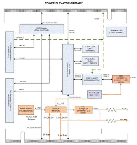
图5.简化TWR-RF框图
MRB-KW01xxyyZZ频段材料清单:
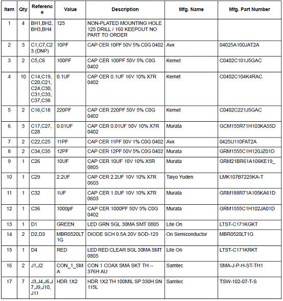
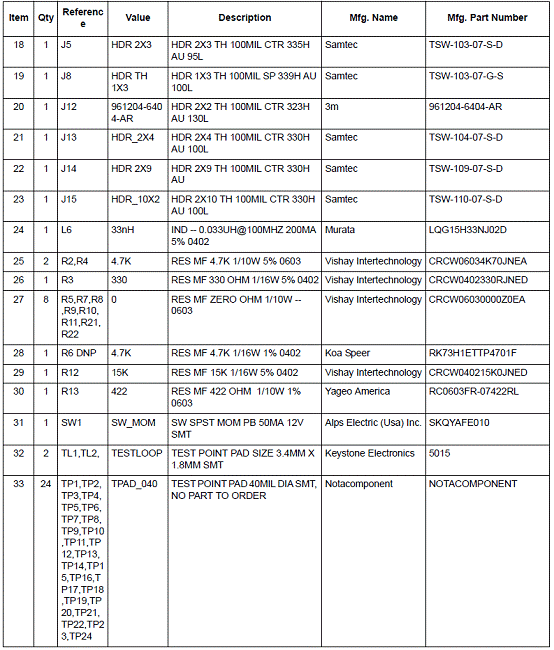
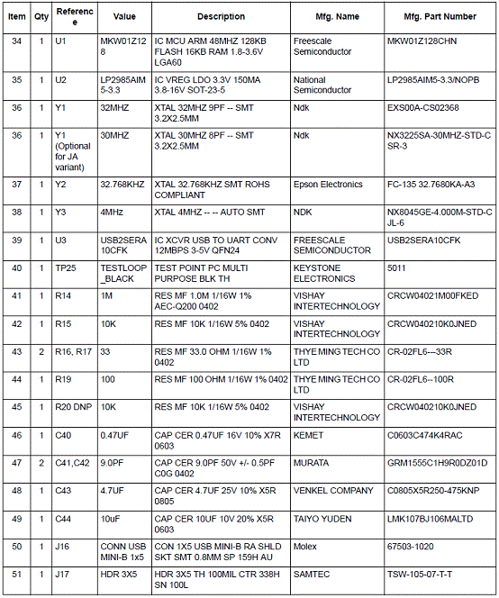
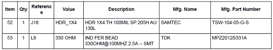
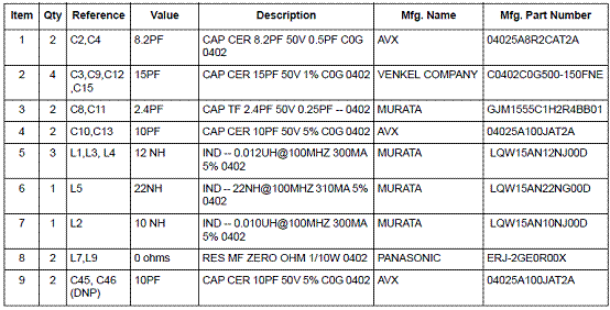
MRB-KW0190yyZZ频段材料清单:
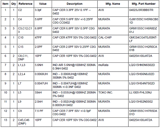
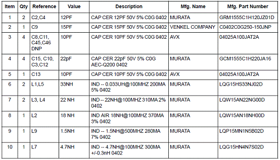
MRB-KW014532CN频段材料清单:
MRB-KW013032CN频段材料清单:
责任编辑:HanFeng
【免责声明】
1、本文内容、数据、图表等来源于网络引用或其他公开资料,版权归属原作者、原发表出处。若版权所有方对本文的引用持有异议,请联系拍明芯城(marketing@iczoom.com),本方将及时处理。
2、本文的引用仅供读者交流学习使用,不涉及商业目的。
3、本文内容仅代表作者观点,拍明芯城不对内容的准确性、可靠性或完整性提供明示或暗示的保证。读者阅读本文后做出的决定或行为,是基于自主意愿和独立判断做出的,请读者明确相关结果。
4、如需转载本方拥有版权的文章,请联系拍明芯城(marketing@iczoom.com)注明“转载原因”。未经允许私自转载拍明芯城将保留追究其法律责任的权利。
拍明芯城拥有对此声明的最终解释权。
相关资讯
:
基于MC33771主控芯片的新能源锂电池管理系统解决方案

AMIC110 32位Sitara ARM MCU开发方案

基于AMIC110多协议可编程工业通信处理器的32位Sitara ARM MCU开发方案

基于展讯SC9820超低成本LTE芯片平台的儿童智能手表解决方案

基于TI公司的AM437x双照相机参考设计

基于MTK6580芯片的W2智能手表解决方案


 2012- 2022 拍明芯城ICZOOM.com 版权所有 客服热线:400-693-8369 (9:00-18:00)


