


 产品分类
产品分类
基于Microchip公司的MCP19118数控模拟电源解决方案
 94
94
 拍明
拍明
原标题:Microchip MCP19118数控模拟电源解决方案
microchip公司的MCP19118/19是高度集成的混合信号模拟PWM电流模式控制器,并集成了用于DC/DC降压应用的微控制器核. 同步降压器输入电压4.5V-40V,输出电压0.5V-3.6V,开关频率100kHz到1.6MHz.PIC MCU核提供完整的定制化工作参数,起动和关断性能,保护级别和故障处理程序.主要用在标准电源转换,LED驱动器,电池充电等.本文介绍了 MCP19118/19同步降压和MCU核的主要特性,框图,微控制器核框图和应用电路,以及MCP19111 评估板主要特性,电路图,材料清单和PCB设计图.
The MCP19118/19 is a highly integrated, mixed signal, analog pulse-width modulation (PWM) current mode controller with an integrated microcontroller core for synchronous DC/DC step-down applications. Since the MCP19118/19 uses traditional analog control circuitry to regulate the output of the DC/DC converter, the integration of the PIC® microcontroller mid-range core is used to provide complete customization of device operating parameters, start-up and shutdown profiles, protection levels and fault handling procedures.
The MCP19118/19 is designed to efficiently operate from a single 4.5V to 40V supply. It features integrated synchronous drivers, bootstrap device, internal linear regulator and 4 kW nonvolatile memory, all in a space-saving 24-pin 4 mm x 4 mm QFN package (MCP19118) or 28-pin 5 mm x 5 mm QFN package (MCP19119).
After initial device configuration using Microchip’s MPLAB® X Integrated Development Environment (IDE) software, the PMBus or I2C can be used by a host to communicate with, or modify, the operation of the MCP19118/19.
Two internal linear regulators generate two 5V rails. One 5V rail is used to provide power for the internal analog circuitry and is contained on-chip. The second 5V rail provides power to the PIC device and is present on the VDD pin. It is recommended that a 1 μF capacitor be placed between VDD and PGND. The VDD pin may also be directly connected to the VDR pin or connected through a low-pass RC filter. The VDR pin provides power to the internal synchronous driver.
MCP19118/19同步降压主要特性:
• Input Voltage: 4.5V to 40V
• Output Voltage: 0.5V to 3.6V
- Greater than 3.6V requires external divider
• Switching Frequency: 100 kHz to 1.6 MHz
• Quiescent Current: 5 mA Typical
• High-Drive:
- +5V Gate Drive
- 1A/2A Source Current
- 1A/2A Sink Current
• Low-Drive:
- +5V Gate Drive
- 2A Source Current
- 4A Sink Current
• Peak Current Mode Control
• Differential Remote Output Sense
• QEC-100 Qualified
• Multiple Output Systems:
- Master or Slave
- Frequency Synchronized
• Configurable Parameters:
- Overcurrent Limit
- Input Undervoltage Lockout
- Output Overvoltage
- Output Undervoltage
- Internal Analog Compensation
- Soft Start Profile
- Synchronous Driver Dead Time
- Switching Frequency
• Thermal Shutdown
MCP19118/19 MCU主要特性:
• Precision 8 MHz Internal Oscillator Block:
- Factory Calibrated
• Interrupt Capable
- Firmware
- Interrupt-on-Change Pins
• Only 35 Instructions to Learn
• 4096 Words On-Chip Program Memory
• High-Endurance Flash:
- 100,000 Write Flash Endurance
- Flash Retention: >40 years
• Watchdog Timer (WDT) with Independent
Oscillator for Reliable Operation
• Programmable Code Protection
• In-Circuit Debug (ICD) via Two Pins (MCP19119)
• In-Circuit Serial Programming™ (ICSP™) via Two Pins
• 11 I/O Pins and One Input-Only Pin (MCP19118)
- Three Open-Drain Pins
• 14 I/O Pins and One Input-Only Pin (MCP19119)
- Three Open-Drain Pins
• Analog-to-Digital Converter (ADC):
- 10-Bit Resolution
- 12 Internal Channels
- Eight External Channels
• Timer0: 8-Bit Timer/Counter with 8-Bit Prescaler
• Enhanced Timer1:
- 16-Bit Timer/Counter with Prescaler
- Two Selectable Clock Sources
• Timer2: 8-Bit Timer/Counter with Prescaler
- 8-Bit Period Register
• I2CTM Communication:
- 7-Bit Address Masking
- Two Dedicated Address Registers
- SMBus/PMBusTM Compatibility
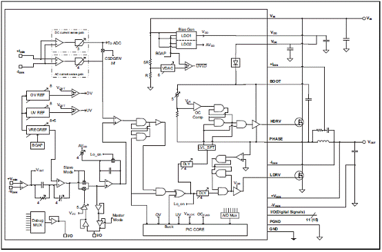
图1. MCP19118/19框图

图2. MCP19118/19微控制器核框图
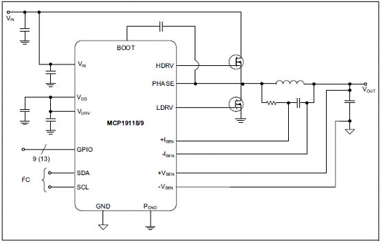
图3. MCP19118/19典型应用电路图
MCP19111 评估板
The MCP19111 is a digitally-enhanced PWM controller. It combines a pure-analog PWM controller with a supervisory microcontroller making it a fast, cost-effective, and configurable power conversion solution. The MCP19111 is ideal for standard power conversion, LED drivers, and battery charging applications. The MCP19111 Evaluation Board demonstrates how the MCP19111 device operates in a synchronous buck topology over a wide input voltage and load range. Nearly all operational and control system parameters are programmable by utilizing the integrated PIC microcontroller core. MPLAB X IDE can be used in conjunction with a Graphical User Interface (GUI) plug-in to easily configure the MCP19111. Alternatively, the user can program the MCP19111 using their own firmware, tailoring it to their application. The evaluation board contains headers for ICSP™ (In-Circuit Serial Programming™) as well as I2C communication, pull-up and pull-down resistor pads and test point pads on each GPIO pin, and two push buttons for system development
The MCP19111 Evaluation Board demonstrates how the MCP19111 device operates in a synchronous buck topology over a wide input voltage and load range. Nearly all operational and control system parameters are programmable by utilizing the integrated PIC microcontroller core. MPLAB X IDE can be used in conjunction with a Graphical User Interface (GUI) plug-in to easily configure the MCP19111. For more information regarding the GUI plug-in, refer to the “MCP19111 MPLAB® X Integrated Development Environment Plug-in User’s Guide” (DS52113). Alternatively, the user can program the MCP19111 using their own firmware, tailoring it to their application. The evaluation board contains headers for ICSP™ (In-Circuit Serial Programming™) as well as I2C communication, pull-up and pull-down resistor pads and test point pads on each GPIO pin, and two push buttons for system development. The MCP19111 Evaluation Board is also intended to demonstrate an optimized Printed Circuit Board (PCB) layout that minimizes parasitics while increasing efficiency and power density.
Proper PCB layout is critical to achieve optimum MCP19111 operation, as well as power train efficiency and noise minimization. MPLAB X IDE, the MCP19111 GUI plug-in, and example firmware is available for download from the Microchip website.
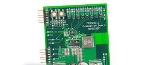
图4.MCP19111 评估板外形图
MCP19111 评估板主要特性:
The MCP19111 Evaluation Board provides the user with an example of an optimized PCB layout which reduces parasitics and increases power density. Some features of this board design include:
• Wide, short traces used to connect power components
• Ceramic VIN capacitors placed as close to the drain of the high-side MOSFET as possible, and as close to the source of the low-side MOSFET as possible
• Split ground plane to decouple the digital and power ground signals
• Careful placement of current sense components to reduce PCB induced noise
Vin range: 5V to 12V
Adjustable Vout range: 0.5V to 3.6V
Maximum output current: 30A with proper air flow
Programming and I2C communication headers
Factory programmed to produce 1.8V from 12V source
The factory programmed source code is available
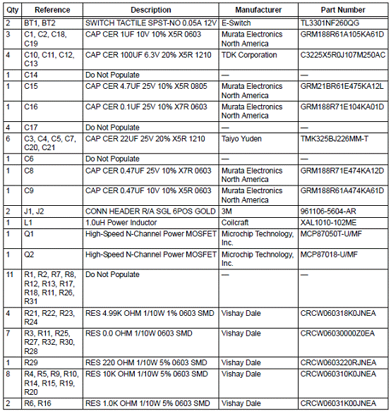
MCP19111 评估板材料清单:

责任编辑:HanFeng
【免责声明】
1、本文内容、数据、图表等来源于网络引用或其他公开资料,版权归属原作者、原发表出处。若版权所有方对本文的引用持有异议,请联系拍明芯城(marketing@iczoom.com),本方将及时处理。
2、本文的引用仅供读者交流学习使用,不涉及商业目的。
3、本文内容仅代表作者观点,拍明芯城不对内容的准确性、可靠性或完整性提供明示或暗示的保证。读者阅读本文后做出的决定或行为,是基于自主意愿和独立判断做出的,请读者明确相关结果。
4、如需转载本方拥有版权的文章,请联系拍明芯城(marketing@iczoom.com)注明“转载原因”。未经允许私自转载拍明芯城将保留追究其法律责任的权利。
拍明芯城拥有对此声明的最终解释权。
相关资讯
:
基于MC33771主控芯片的新能源锂电池管理系统解决方案

AMIC110 32位Sitara ARM MCU开发方案

基于AMIC110多协议可编程工业通信处理器的32位Sitara ARM MCU开发方案

基于展讯SC9820超低成本LTE芯片平台的儿童智能手表解决方案

基于TI公司的AM437x双照相机参考设计

基于MTK6580芯片的W2智能手表解决方案


 2012- 2022 拍明芯城ICZOOM.com 版权所有 客服热线:400-693-8369 (9:00-18:00)


