


 产品分类
产品分类
基于TI的LMT70+MSP430F5529可穿戴设备温度传感器参考设计
 388
388
 拍明
拍明
原标题:TI LMT70+MSP430F5529可穿戴设备温度传感器参考设计
TI LMT70+MSP430F5529可穿戴设备温度传感器参考设计
TI的可穿戴设备温度传感器参考设计采用超小型高精度低功耗CMOS模拟温度传感器LMT70和超低功耗MCU MSP430F5529.LMT70的精度0.13C,小型的WCSP封装,具有很快的热响应时间,非常适合人体温度测量,很适合于用在可穿戴市场.
The LMT70 is an ultra-small, high-precision, low-power CMOS analog temperature sensor with an output enable pin. Applications for the LMT70 include virtually any type of temperature sensing where cost-effective, high precision and low-power are required, such as Internet of Things (IoT) sensor nodes, medical thermometers, high-precision instrumentation and battery powered devices. The LMT70 is also a great replacement for RTD and precision NTC/PTC thermistors.
Its output enable pin allows multiple LMT70s to share one ADC channel, thus simplifying ADC calibration and reducing the overall system cost for precision temperature sensing. The LMT70 also has a linear and low impedance output allowing seamless interface to an off-the-shelf MCU/ADC. Dissipating less than 36µW, the LMT70 has ultra-low self-heating supporting its high-precision over a wide temperature range.
The LMT70A provides unparalleled temperature matching performance of 0.1°C (max) for two adjacent LMT70A’s picked from the same tape and reel. Therefore, the LMT70A is an ideal solution for energy metering applications requiring heat transfer calculations.
LMT70主要特性:
Accuracy:
±0.05℃ (typ) or ±0.13℃ (max) at 30℃
±0.2℃ (max) from 20℃ to 90℃
±0.23℃ (max) from 90℃ to 110℃
±0.36℃ (max) from –55℃ to 150℃
Wide Temperature Range: −55℃ to 150℃
Matching of Two Adjacent LMT70A on Tape and Reel: 0.1℃ (max) at 30℃
Very Linear Analog Temperature Sensor with Output Enable Pin
NTC Output Slope: –5.19 mV/℃
Output On/Off Switch with RDS on< 80 Ω
Wide Power Supply Range: 2.0 V to 5.5 V
Low Power Supply Current: 12 µA (max)
Ultra Small 0.88 mm by 0.88 mm 4-bump WLCSP (Ball Grid) Package
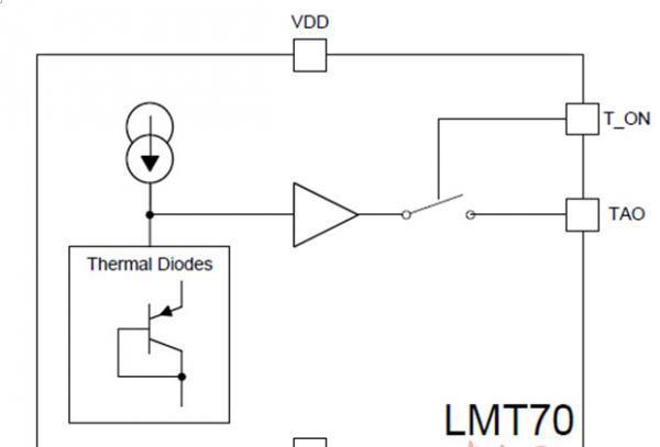
图1.LMT70框图
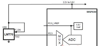
图2.LMT70典型应用电路图
The Texas Instruments MSP430 family of ultralow-power microcontrollers consists of several devices featuring different sets of peripherals targeted for various applications. The architecture, combined with extensive low-power modes, is optimized to achieve extended battery life in portable measurement applications. The device features a powerful 16-bit RISC CPU, 16-bit registers, and constant generators that contribute to maximum code efficiency. The digitally controlled oscillator (DCO) allows wake-up from low-power modes to active mode in 3.5 µs (typical).
The MSP430F5529, MSP430F5527, MSP430F5525, and MSP430F5521 are microcontroller configurations with integrated USB and PHY supporting USB 2.0, four 16-bit timers, a high-performance 12-bit analog-to-digital converter (ADC), two universal serial communication interfaces (USCI), hardware multiplier, DMA, real-time clock module with alarm capabilities, and 63 I/O pins. The msp430f5528, MSP430F5526, MSP430F5524, and MSP430F5522 include all of these peripherals but have 47 I/O pins.
The MSP430F5519, MSP430F5517, and MSP430F5515 are microcontroller configurations with integrated USB and PHY supporting USB 2.0, four 16-bit timers, two universal serial communication interfaces (USCI), hardware multiplier, DMA, real time clock module with alarm capabilities, and 63 I/O pins. The MSP430F5514 and MSP430FF5513 include all of these peripherals but have 47 I/O pins.
Typical applications include analog and digital sensor systems, data loggers, and others that require connectivity to various USB hosts.
MSP430F5529主要特性:
Low Supply-Voltage Range: 3.6 V Down to 1.8 V
Ultralow Power Consumption
Active Mode (AM):
All System Clocks Active
290 µA/MHz at 8 MHz, 3.0 V, Flash Program Execution (Typical)
150 µA/MHz at 8 MHz, 3.0 V, RAM Program Execution (Typical)
Standby Mode (LPM3):
Real-Time Clock With Crystal, Watchdog, and Supply Supervisor Operational, Full RAM Retention, Fast Wake-Up:
1.9 µA at 2.2 V, 2.1 µA at 3.0 V (Typical)
Low-Power Oscillator (VLO), General-Purpose Counter, Watchdog, and Supply Supervisor Operational, Full RAM Retention, Fast Wake-Up:
1.4 µA at 3.0 V (Typical)
Off Mode (LPM4):
Full RAM Retention, Supply Supervisor Operational, Fast Wake-Up:
1.1 µA at 3.0 V (Typical)
Shutdown Mode (LPM4.5):
0.18 µA at 3.0 V (Typical)
Wake-Up From Standby Mode in 3.5 µs (Typical)
16-Bit RISC Architecture, Extended Memory, up to 25-MHz System Clock
Flexible Power Management System
Fully Integrated LDO With Programmable Regulated Core Supply Voltage
Supply Voltage Supervision, Monitoring, and Brownout
Unified Clock System
FLL Control Loop for Frequency Stabilization
Low-Power Low-Frequency Internal Clock Source (VLO)
Low-Frequency Trimmed Internal Reference Source (REFO)
32-kHz Watch Crystals (XT1)
High-Frequency Crystals up to 32 MHz (XT2)
16-Bit Timer TA0, Timer_AWith Five Capture/Compare Registers
16-Bit Timer TA1, Timer_AWith Three Capture/Compare Registers
16-Bit Timer TA2, Timer_AWith Three Capture/Compare Registers
16-Bit Timer TB0, Timer_BWith Seven Capture/Compare Shadow Registers
Two Universal Serial Communication Interfaces
USCI_A0 and USCI_A1 Each Support: Enhanced UART Supports Auto-Baudrate Detection, IrDA Encoder and Decoder, Synchronous SPI
USCI_B0 and USCI_B1 Each Support: I2CTM, Synchronous SPI
Full-Speed Universal Serial Bus (USB)
Integrated USB-PHY
Integrated 3.3-V and 1.8-V USB Power System
Integrated USB-PLL
Eight Input, Eight Output Endpoints
12-Bit Analog-to-Digital (A/D) Converter (MSP430F552x Only) With Internal Reference, Sample-and-Hold, and Autoscan Feature
Comparator
Hardware Multiplier Supporting 32-Bit Operations
Serial Onboard Programming, No External Programming Voltage Needed
Three Channel Internal DMA
Basic Timer With Real-Time Clock Feature
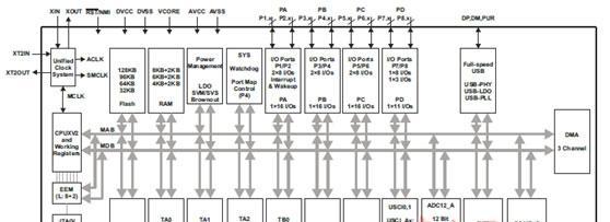
图3.MSP430F5529IPN/5527IPN/5525IPN/F5521IPN功能框图
可穿戴设备温度传感器参考设计
This TI Design is to demonstrate temperature sensoring aimed at the wearables market. The LMT70 temperature sensor is ideal for wearable devices due to its 0.13C temperature accuracy at human body temperatures. Its small form WCSP package allows it to be heated up quickly and thus have a fast thermal response time when placed onto a human body.
可穿戴设备温度传感器参考设计主要特性:
USB form factor PCB board with breakout tabs to attach different substrates
TI Design report includes thermal response of different substrates and MSP430F5528 ADC calibration techniques.
This TI Design system is tested and includes firmware, GUI, User Guides, and a Test Report

图4.可穿戴设备温度传感器参考设计外形图
责任编辑:HanFeng
【免责声明】
1、本文内容、数据、图表等来源于网络引用或其他公开资料,版权归属原作者、原发表出处。若版权所有方对本文的引用持有异议,请联系拍明芯城(marketing@iczoom.com),本方将及时处理。
2、本文的引用仅供读者交流学习使用,不涉及商业目的。
3、本文内容仅代表作者观点,拍明芯城不对内容的准确性、可靠性或完整性提供明示或暗示的保证。读者阅读本文后做出的决定或行为,是基于自主意愿和独立判断做出的,请读者明确相关结果。
4、如需转载本方拥有版权的文章,请联系拍明芯城(marketing@iczoom.com)注明“转载原因”。未经允许私自转载拍明芯城将保留追究其法律责任的权利。
拍明芯城拥有对此声明的最终解释权。
相关资讯
:
基于MC33771主控芯片的新能源锂电池管理系统解决方案

AMIC110 32位Sitara ARM MCU开发方案

基于AMIC110多协议可编程工业通信处理器的32位Sitara ARM MCU开发方案

基于展讯SC9820超低成本LTE芯片平台的儿童智能手表解决方案

基于TI公司的AM437x双照相机参考设计

基于MTK6580芯片的W2智能手表解决方案


 2012- 2022 拍明芯城ICZOOM.com 版权所有 客服热线:400-693-8369 (9:00-18:00)


