基于Renesas公司的RX200系列MCU 3D打印机解决方案
 171
171
 拍明
拍明
原标题:Renesas RX200系列MCU 3D打印机解决方案
Renesas公司的RX200系列mcu基于32位RX CPU核,工作频率50MHz时的性能高达78 DMIPS,单电源1.62-V到5.5-V工作,高达1MB闪存,12位ADC和10位DAC,集成了ELC,MPC,RTC和多达15路通信通路以及和IEC60730兼容的功能,主要用在通用工业和消费类设备.本文介绍了RX200系列主要特性和框图,入门套件RSKRX210B主要特性,框图,PCB元件分布图,电路图以及3D打印机系统框图.
The extreme evolution to embedded systems led by Renesas’ new RX MCU family. Equipped with a new-generation core, the RX family can respond to the ever-increasing demands and challenges on the MCUs of today and tomorrow.
Even higher performance, greater code efficiency, lower power consumption, and more integration have been achieved, while providing legacy, enhanced and new peripheral functions for many applications.
The low power series of the RX Family. The RX200 product series combines the high calculation performance of the RX600 and new low power and safety capabilities.
RX200系列主要特性:
■ 32-bit RX CPU core
Max.operating frequency: 50 MHzCapable of 78 DMIPS in operation at 50 MHz
Accumulator handles 64-bit results (for a single instruction)from 32- × 32-bit operations
Multiplication and division unit handles 32- × 32-bitoperations (multiplication instructions take one CPU clockcycle)
Fast interrupt
CISC Harvard architecture with 5-stage pipeline
Variable-length instructions, ultra-compact code
On-chip debugging circuit
■ Low power design and architecture
Operation from a single 1.62-V to 5.5-V supply
1.62-V operation available (at up to 20 MHz)
Deep software standby mode with RTC remaining usable
Four low power consumption modes
■ On-chip flash memory for code, no wait states
50-MHz operation, 20-ns read cycle
No wait states for reading at full CPU speed
64-K to 1-Mbyte capacities
User code programmable via the SCI
Programmable at 1.62 V
For instructions and operands
■ On-chip data flash memory
8 Kbytes(Number of times of reprogramming: 100,000)
Erasing and programming impose no load on the CPU.
■ On-chip SRAM, no wait states
12-K to 96-Kbyte size capacities
■ DMA
DMAC: Incorporates four channels
DTC: Four transfer modes
■ ELC
Module operation can be initiated by event signals withoutgoing through interrupts.
Modules can operate while the CPU is sleeping.
■ Reset and supply management
Nine types of reset, including the power-on reset (POR)
Low voltage detection (LVD) with voltage settings
■ Clock functions
Frequency of external clock: Up to 20 MHz
Frequency of the oscillator for sub-clock generation: 32.768kHz
PLL circuit input: 4 MHz to 12.5 MHz
On-chip low- and high-speed oscillators, dedicated on-chiplow-speed oscillator for the IWDT
Generation of a dedicated 32.768-kHz clock for the RTC
Clock frequency accuracy measurement circuit (CAC)
■ Realtime clock
Adjustment functions (30 seconds, leap year, and error)
Year and month display or 32-bit second display (binarycounter) is selectable
Time capture function
Time capture on event-signal input through external pins
RTC capable of initiating return from deep software standbymode
■ Independent watchdog timer
125-kHz on-chip oscillator produces a dedicated clock signalto drive IWDT operation
■ Useful functions for IEC60730 compliance
Self-diagnostic and disconnection-detection assistancefunctions for the A/D converter, clock frequency accuracymeasurement circuit, independent watchdog timer, functionsto assist in RAM testing, etc.
■ Up to 15 communications channels
SCI with many useful functions (up to 13 channels)
Asynchronous mode, clock synchronous mode, smart cardinterface
I2C bus interface: Transfer at up to 400 kbps, capable ofSMBus operation (one channel)
RSPI (one channel): Transfer at up to 16 Mbps (768-Kbyte/1-Mbyte flash memory or 144/145-pin products)
■ External address space
Four CS areas (4 × 16 Mbytes)
8- or 16-bit bus space is selectable per area
■ Up to 20 extended-function timers
16-bit MTU: input capture, output compare, complementaryPWM output, phase counting mode(six channels)
16-bit TPU: input capture, output capture, phase countingmode (six channels)
8-bit TMR (four channels)
16-bit compare-match timers (four channels)
■ 12-bit A/D converter
Capable of conversion within 1 μs
Sample-and-hold circuits (for three channels)
Three-channel synchronized sampling available
Self-diagnostic function and analog input disconnectiondetection assistance function
■ 10-bit D/A converter
■ Analog comparator
■ General I/O ports
5-V tolerant, open drain, input pull-up, switching of drivingability
■ MPC
Multiple locations are selectable for I/O pins of peripheralfunctions
■ Temperature sensor
■ Operating temp.range
40℃ to +85℃
40℃ to +105℃
■ Applications
69WLBGA (SWBG0069LA-A): General consumerequipment
Other than above package: General industrial and consumerEquipment

图1。RX200系列框图
入门套件RSKRX210B
The Renesas Starter Kit for RX210 (B Mask) is intended as a user-friendly introductory and evaluation tool for the RX210 microcontroller. The board also provides a useful platform for evaluating the Renesas suite of development tools for coding and debugging, using High-performance Embedded Workshop*1 as well as programming the device using E1 emulator and/or Flash Development Toolkit.
The Renesas Starter Kit for RX210 (B Mask) may be connected to the host PC using a simple RS232 serial connection or via the included USB E1 on chip debugging interface.
The purpose of the board is to enable the user to evaluate the capabilities of the device and its peripherals by giving the user a simple platform on which code can be run only minutes from opening box. It can also prove an invaluable tool in development by providing a useful test platform for code already debugged using one of our more powerful emulation tools.

图2.入门套件RSKRX210B外形图
入门套件RSKRX210B包括:
CPU Board
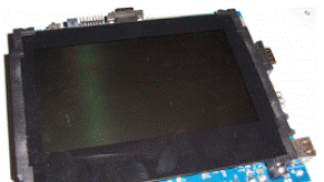
Detachable LCD Display Module
Detachable AD Adjustment Shaft
E1 Emulator
Connection Cable (USB Cable, User Interface Cable)
Quick Start Guide
CD-ROM
- Documents: User Manual, Tutorial, and more
- IDE: High-performance Embedded Workshop
- C Compiler: C/C++ Compiler Package for RX Family Evaluation Version
- Debugger: E1/E20 Emulator Debugger
入门套件RSKRX210B主要特性:
• Renesas microcontroller programming
• User code debugging
• User circuitry such as switches, LEDs and a potentiometer
• Sample application
• Sample peripheral device initialisation code

图3.入门套件RSKRX210B框图

图4.入门套件RSKRX210B元件布局图

图5.入门套件RSKRX210B顶层元件分布图
3D打印机
3D printers are attracting attention as the prices of personal hobby use low-cost versions drop. Many low-cost 3D printers use the Fused Deposition Modeling method and control 3D coordinates by controlling a plastic outputting head in 2D coordinates and controlling the height of the stage. A plastic loader motor and a cooling fan motor also require PWM output. In addition, large-capacity flash ROM and a high-performance CPU are required for high-speed processing of large volume data. Also required are serial I/O for receiving date from a PC via USB or flash memory media devices and controlling LCD panel modules.
Renesas Electronics offers the RX200 Series, which has a high-performance CPU, PWM for controlling stepper motors and serial I/O for communicating with various peripheral devices, and the RX600 Series, which has an RSPI for controlling serial flash as well as semiconductor devices such as an LED driver IC, op-amp and reset IC for 3D printers.
System Block Diagram

责任编辑:HanFeng
【免责声明】
1、本文内容、数据、图表等来源于网络引用或其他公开资料,版权归属原作者、原发表出处。若版权所有方对本文的引用持有异议,请联系拍明芯城(marketing@iczoom.com),本方将及时处理。
2、本文的引用仅供读者交流学习使用,不涉及商业目的。
3、本文内容仅代表作者观点,拍明芯城不对内容的准确性、可靠性或完整性提供明示或暗示的保证。读者阅读本文后做出的决定或行为,是基于自主意愿和独立判断做出的,请读者明确相关结果。
4、如需转载本方拥有版权的文章,请联系拍明芯城(marketing@iczoom.com)注明“转载原因”。未经允许私自转载拍明芯城将保留追究其法律责任的权利。
拍明芯城拥有对此声明的最终解释权。


 产品分类
产品分类




 2012- 2022 拍明芯城ICZOOM.com 版权所有 客服热线:400-693-8369 (9:00-18:00)


