


 产品分类
产品分类
基于NXP的SSL5511T 60W(145 V-400 mA)LED驱动方案
 125
125
 拍明
拍明
原标题:NXP SSL5511T 60W(145 V-400 mA)LED驱动方案
nxp公司的SSL5511T是离线可调光LED控制器,支持反激,降压和降压-升压拓扑,可选择低THD或低LED电流波纹模式,模拟IEC60929输入或数字控制输入调光,集成了起动JFET,具有多种保护,主要用在100 V (AC), 120 V (AC)和230 V (AC) LED照明.本文介绍了SSL5511T主要特性和优势,框图,反激应用电路,以及演示板SSL5511DB1274主要特性,电路图和材料清单.
The SSL5511T is an offline dimmable controller IC, intended to drive dimmable LEDs ingeneral lighting applications, like remote-controlled luminaires and smart lamps.
The main benefits of this IC include:
• Dim level control with either an analog or a digital control input
• Selectable modes for high power factor or low ripple, allowing a wide LED power range
• Large dimming range
• Single stage topology for small PCB footprint
• Ease of design-in
• Integrated start-up JFET
• Low electronic Bill Of Material (BOM)
• Various converter topologies supported
The IC drives an external switch for easy power scaling. It has been designed to start updirectly from the High-Voltage (HV) supply by an internal high-voltage current source.
Flyback, buck and buck-boost circuit topologies are supported. Primary side sensingprovides accurate output current control.
The IC can detect analog signals (according to IEC60929 annex E) or digital controlsignals and translate them to a continuous LED current in multiple ways. It can operate inthree switching modes at two switching frequency ranges. It offers tradeoffs between theoutput current ripple, the mains current Total Harmonic Distortion (THD) and theapplication size. The IC incorporates all required protection features.
SSL5511T主要特性和优势:
LED controller IC for driving strings of LEDs or high-voltage LEDs from rectified mains
High-efficiency switch mode buck, flyback or buck-boost controller driving an external power FET
Two maximum switching frequencies for highest efficiency or smallest applicationsize
Zero current switching at switch turn-on
Zero voltage or valley switching at switch turn-on
Selectable low THD or low LED current ripple modes
Analog IEC60929 input or digital control input for dimming
Continuous (analog) regulation of LED current in both the dimming control modes
Dim curve selection based on the control input type
No binning on LED forward voltage required
LED current accuracy within ±4 % across variations in components and conditions
Built-in Protections:
UnderVoltageLockOut (UVLO)
Leading Edge Blanking (LEB)
OverCurrent Protection (OCP)
Internal OverTemperature Protection (OTP)
Brownout protection
Output Short Protection (OSP)
Output open OverVoltage Protection (OVP)
Mains synchronization loss protection
Low component count LED driver solution
Compatible with wall switches with built-in indication light during standby(
IC lifetime matches or surpasses LED lamp lifetime
SSL5511T应用:
Compact mains connected, remote-controlled LED lamps with accurate, dimmablecurrent output for single or universal mains voltages, including 100 V (AC), 120 V (AC)and 230 V (AC). External components determine the power level. The power levelranges from 4 W to over 25 W. Applications fit in common form factors like PAR,GU10, A19, and the candle form factor.
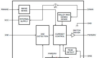
图1.SSL5511T框图

图2.SSL5511T反激应用电图:LTHD;输入= 230 V (AC);输出= 35 V/200 mA
演示板SSL5511DB1274
The SSL5511T is a high-efficient analog/PWM dimmable controller IC for LED solutions. The SSL5511DB1274 demo board is a single PCB dimmable LED driver example of a non-isolated buck-boost stage.
The SSL5511DB1274 demo board drives a constant current through the LEDs from a rectified 230 V or 277 V mains input voltage. This 60 W demo board is optimized for a LED string voltage of approx. 145 V at 400 mA. The design and the components used are optimized for single sided SMD only PCB design. The application is tailored for streetlight applications.
The solution is documented as a "design prototype" in Solution Brief SB00005.

图3.演示板SSL5511DB1274外形图
演示板SSL5511DB1274主要特性:
Single PCB with LED and SMPS converter enabling high reliability and low production costs
SMD only PCB design enabling full automatic component placement
Single layer FR4 PCB, 120 x 240 mm, 70 um copper thickness
Efficient non-isolated buck-boost QR topology
230 and 277 VAC input voltage
Short turn-on delay time
Low mains current harmonics
Low output ripple filter
1 V to 10 V dimmable when using SSL5511T
Non dimmable option when using SSL5101T
3 x series x 10 parallel output LEDs
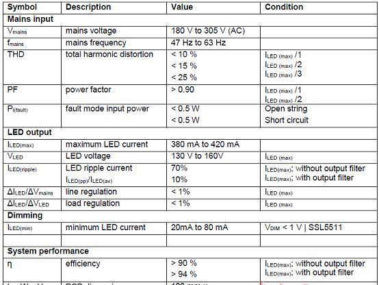
演示板SSL5511DB1274指标:
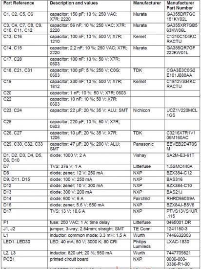
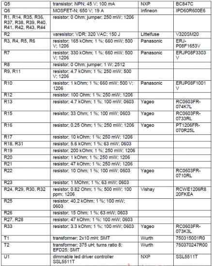
演示板SSL5511DB1274材料清单:
责任编辑:HanFeng
【免责声明】
1、本文内容、数据、图表等来源于网络引用或其他公开资料,版权归属原作者、原发表出处。若版权所有方对本文的引用持有异议,请联系拍明芯城(marketing@iczoom.com),本方将及时处理。
2、本文的引用仅供读者交流学习使用,不涉及商业目的。
3、本文内容仅代表作者观点,拍明芯城不对内容的准确性、可靠性或完整性提供明示或暗示的保证。读者阅读本文后做出的决定或行为,是基于自主意愿和独立判断做出的,请读者明确相关结果。
4、如需转载本方拥有版权的文章,请联系拍明芯城(marketing@iczoom.com)注明“转载原因”。未经允许私自转载拍明芯城将保留追究其法律责任的权利。
拍明芯城拥有对此声明的最终解释权。
相关资讯
:
基于MC33771主控芯片的新能源锂电池管理系统解决方案

AMIC110 32位Sitara ARM MCU开发方案

基于AMIC110多协议可编程工业通信处理器的32位Sitara ARM MCU开发方案

基于展讯SC9820超低成本LTE芯片平台的儿童智能手表解决方案

基于TI公司的AM437x双照相机参考设计

基于MTK6580芯片的W2智能手表解决方案


 2012- 2022 拍明芯城ICZOOM.com 版权所有 客服热线:400-693-8369 (9:00-18:00)


