


 产品分类
产品分类
基于ST公司的STM32L151 32位MCU蓝牙低功耗(BLE)开发方案
 469
469
 拍明
拍明
原标题:ST STM32L151 32位MCU蓝牙低功耗(BLE)开发方案
ST公司的stm32L151VD-X和STM32L152VD-X是基于高性能ARM® Cortex®-M3 32位RISC内核的超低功耗MCU,工作频率32MHz(33.3DMIPS),集成了存储器保护单元(MPU),高速嵌入存储器(闪存高达384KB,RAM高达80KB),以及广泛的增强的I/O和连接到两条APB总线的外设.本文介绍了STM32L151VD-X和STM32L152VD-X主要特性,框图,以及蓝牙低功耗(BLE)评估板X-NUCLEO-IDB04A1主要特性,框图,电路图和材料清单.
The ultra-low-power STM32L151VD-X and STM32L152VD-X devices incorporate the connectivity power of the universal serial bus (USB) with the high-performance ARM® Cortex®-M3 32-bit RISC core operating at a frequency of 32 MHz (33.3 DMIPS), a memory protection unit (MPU), high-speed embedded memories (Flash memory up to 384 Kbytes and RAM up to 80 Kbytes), and an extensive range of enhanced I/Os and peripherals connected to two APB buses.
The STM32L151VD-X and STM32L152VD-X devices offer two operational amplifiers, one 12-bit ADC, two DACs, two ultra-low-power comparators, one general-purpose 32-bit timer, six general-purpose 16-bit timers and two basic timers, which can be used as time bases.
Moreover, the STM32L151VD-X and STM32L152VD-X devices contain standard and advanced communication interfaces: up to two I2Cs, three SPIs, two I2S, three USARTs, two UARTs and an USB. The STM32L151VD-X and STM32L152VD-X devices offer up to 23 capacitive sensing channels to simply add a touch sensing functionality to any application.
They also include a real-time clock and a set of backup registers that remain powered in Standby mode.
Finally, the integrated LCD controller (except STM32L151VD-X) has a built-in LCD voltage generator that allows to drive up to 8 multiplexed LCDs with the contrast independent of the supply voltage.
The ultra-low-power STM32L151VD-X and STM32L152VD-X devices operate from a 1.8 to 3.6 V power supply (down to 1.65 V at power down) with BOR and from a 1.65 to 3.6 V power supply without BOR option. They are available in the -40 to +85℃ and -40 to +105℃ temperature ranges. A comprehensive set of power-saving modes allows the design of low-power applications.
STM32L151主要特性:
• Ultra-low-power platform
– 1.65 V to 3.6 V power supply
– -40℃ to 105℃ temperature range
– 290 nA Standby mode (3 wakeup pins)
– 1.11 μA Standby mode + RTC
– 560 nA Stop mode (16 wakeup lines)
– 1.4 μA Stop mode + RTC
– 11 μA Low-power run mode down to 4.6 μA in Low-power sleep mode
– 195 μA/MHz Run mode
– 10 nA ultra-low I/O leakage
– 8 μs wakeup time
• Core: ARM® Cortex®-M3 32-bit CPU
– From 32 kHz up to 32 MHz max
– 1.25 DMIPS/MHz (Dhrystone 2.1)
– Memory protection unit
• Up to 23 capacitive sensing channels
• CRC calculation unit, 96-bit unique ID
• Reset and supply management
– Low-power, ultrasafe BOR (brownout reset) with 5 selectable thresholds
– Ultra-low-power POR/PDR
– Programmable voltage detector (PVD)
• Clock sources
– 1 to 24 MHz crystal oscillator
– 32 kHz oscillator for RTC with calibration
– Internal 16 MHz oscillator factory trimmed RC(+/-1%) with PLL option
– Internal low-power 37 kHz oscillator
– Internal multispeed low-power 65 kHz to 4.2 MHz oscillator – PLL for CPU clock and USB (48 MHz)
• Pre-programmed bootloader
– USB and USART supported
• Up to 116 fast I/Os (102 I/Os 5V tolerant), all mappable on 16 external interrupt vectors
• Memories
– 384 KB Flash memory with ECC (with 2 banks of 192 KB enabling RWW capability)
– 80 KB RAM
– 16 KB of true EEPROM with ECC
– 128 byte backup register
• LCD driver (except STM32L151VD-X) up to 8x40 segments, contrast adjustment, blinking mode, step-up converter
• Rich analog peripherals (down to 1.8 V)
– 2x operational amplifiers
– 12-bit ADC 1 Msps up to 40 channels
– 12-bit DAC 2 ch with output buffers
– 2x ultra-low-power comparators (window mode and wakeup capability)
• DMA controller 12x channels
• 11x peripheral communication interfaces
– 1x USB 2.0 (internal 48 MHz PLL)
– 5x USARTs
– Up to 8x SPIs (2x I2S,3x 16 Mbit/s)
– 2x I2Cs (SMBus/PMBus)
• 11x timers: 1x 32-bit, 6x 16-bit with up to 4 IC/OC/PWM channels, 2x 16-bit basic timers, 2x watchdog timers (independent and window)
• Development support: serial wire debug, JTAG and trace

图1.超低功耗STM32L151VD-X和STM32L152VD-X框图

图2.超低功耗STM32L151时钟树图
基于BlueNRG的蓝牙低功耗(BLE)评估板X-NUCLEO-IDB04A1
This document provides detailed hardware requirements and board connections for the XNUCLEO-IDB04A1 Bluetooth® low energy (BLE) evaluation board based on BlueNRG forSTM32 Nucleo. This board is part of STMicroelectronics’offering of evaluation boards designed around the BlueNRG Bluetooth low energy wireless network processor.
The excellent performance of BlueNRG and the best matching between BlueNRG and BALF-NRG-01D3, X-NUCLEO-IDB04A1 passed the RF TEST for Japan Radio Law certification with higher margin above the specification values as well as it is FCC certified
(FCC ID: S9NIDB04A1).
The X-NUCLEO-IDB04A1 is a Bluetooth low energy evaluation board to allow expansion ofthe STM32 Nucleo boards. It is compatible with the Arduino UNO R3 connector layout, andis designed around BlueNRG, a Bluetooth low energy, low power network coprocessorcompliant with BTLE 4.0 and the BALF-NRG-01D3, an ultra-miniature balun optimized forST BlueNRG RF IC, which integrates matching network and harmonics filter. The XNUCLEO-IDB04A1 interfaces with the STM32 MCU via SPI pin, and the user can changethe default SPI clock, the SPI chip select and SPI IRQ by changing one resistor on theevaluation board. The excellent performance of BlueNRG and the best matching betweenBlueNRG and BALF-NRG-01D3, X-NUCLEO-IDB04A1 passed the RF TEST for JapanRadio Law certification with higher margin above the specification values as well as it isFCC certified (FCC ID: S9NIDB04A1).
BLE评估板X-NUCLEO-IDB04A1主要特性:
·BlueNRG low power, low energy Bluetooth network coprocessor
·BALF-NRG-01D3 balun& harmonic filter
·Free comprehensive development firmware library and example for BlueNRG, compatiblewith STM32Cube firmware
·Bluetooth low energy 4.0 master and slave compliant
·Compatible with STM32 Nucleo boards
·Equipped with Arduino UNO R3 connector
·Very low power consumption: 7.3 mA RX and 8.2 mA TX at +0 dBm
·Maximum transmission power: +8 dBm
·Excellent receiver sensitivity (-88 dBm)
·X-NUCLEO-IDB04A1 is FCC certified (FCC ID: S9NIDB04A1)
·X-NUCLEO-IDB04A1 is officially certificated as a BTLE 5 mW module for Japan Radio
Law "TYPE" Certification by Japan government
·RoHS compliant
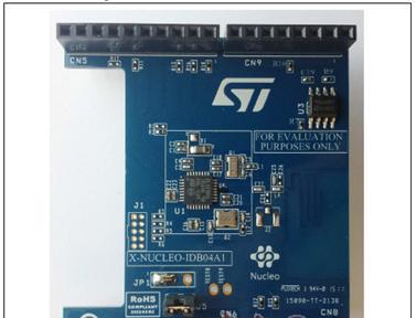
图3.BLE评估板X-NUCLEO-IDB04A1外形图

图4.BLE评估板X-NUCLEO-IDB04A1框图

图5.BLE评估板X-NUCLEO-IDB04A1和STM32 Nucleo板连接图
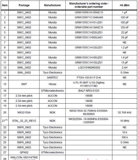
BLE评估板X-NUCLEO-IDB04A1材料清单:

责任编辑:HanFeng
【免责声明】
1、本文内容、数据、图表等来源于网络引用或其他公开资料,版权归属原作者、原发表出处。若版权所有方对本文的引用持有异议,请联系拍明芯城(marketing@iczoom.com),本方将及时处理。
2、本文的引用仅供读者交流学习使用,不涉及商业目的。
3、本文内容仅代表作者观点,拍明芯城不对内容的准确性、可靠性或完整性提供明示或暗示的保证。读者阅读本文后做出的决定或行为,是基于自主意愿和独立判断做出的,请读者明确相关结果。
4、如需转载本方拥有版权的文章,请联系拍明芯城(marketing@iczoom.com)注明“转载原因”。未经允许私自转载拍明芯城将保留追究其法律责任的权利。
拍明芯城拥有对此声明的最终解释权。
相关资讯
:
基于MC33771主控芯片的新能源锂电池管理系统解决方案

AMIC110 32位Sitara ARM MCU开发方案

基于AMIC110多协议可编程工业通信处理器的32位Sitara ARM MCU开发方案

基于展讯SC9820超低成本LTE芯片平台的儿童智能手表解决方案

基于TI公司的AM437x双照相机参考设计

基于MTK6580芯片的W2智能手表解决方案


 2012- 2022 拍明芯城ICZOOM.com 版权所有 客服热线:400-693-8369 (9:00-18:00)


