


 产品分类
产品分类
基于NXP公司的CLRC663无接触读卡器解决方案
 650
650
 拍明
拍明
原标题:NXP CLRC663无接触读卡器解决方案
NXP公司的CLRC663是新一代高性能近距离非接触式读卡器,支持多种协议如MIFARE Classic 1K, MIFARE Classic 4K, MIFARE Ultralight,MIFARE Ultralight C, MIFARE PLUS和MIFARE DESFire,数据速率高达848kbps,适用于银行,电子政务,交通,移动支付等众多基础设施应用.本文介绍了CLRC663主要特性和优势,框图,应用电路以及CLEV663无接触读卡器评估板主要特性,电路图和材料清单.
The CLRC663’s internal transmitter is able to drive a reader/writer antenna designed to communicate with ISO/IEC 14443A/MIFARE cards and transponders without additional active circuitry. The digital module manages the complete ISO/IEC 14443A framing and error detection functionality (parity and CRC).
The CLRC663 supports MIFARE Classic 1K, MIFARE Classic 4K, MIFARE Ultralight,MIFARE Ultralight C, MIFARE PLUS and MIFARE DESFire products. The CLRC663 supports MIFARE higher transfer speeds of up to 848 kbit/s in both directions.
The CLRC663 supports layer 2 and 3 of the ISO/IEC 14443B reader/writercommunication scheme except anticollision. The anticollision needs to be implemented in the firmware of the host controller as well as in the upper layers.
The CLRC663 is able to demodulate and decode FeliCa coded signals.TheFeliCa receiver part provides the demodulation and decoding circuitry for FeliCa coded signals.
The CLRC663 handles the FeliCa framing and error detection such as CRC. The CLRC663 supports FeliCa higher transfer speeds of up to 424 kbit/s in both directions.The CLRC663 is supporting the P2P passive initiator mode in accordance withISO/IEC 18092.
The CLRC663 supports the vicinity protocol according to ISO/IEC15693, EPC UID and ISO/IEC 18000-3 mode 3/ EPC Class-1 HF.
The following host interfaces are supported:
• Serial Peripheral Interface (SPI)
• Serial UART (similar to RS232 with voltage levels dependent on pin voltage supply)
• I2C-bus interface (two versions are implemented: I2C and I2CL)
The CLRC663 supports the connection of a secure access module (SAM). A dedicated separate I2C interface is implemented for a connection of the SAM.
The SAM can be used for high secure key storage and acts as a very performant crypto coprocessor. Adedicated SAM is available for connection to the CLRC663.
The CLRC663 multi-protocol NFC frontend IC supports the following operating modes
• Read/write mode supporting ISO/IEC 14443A/MIFARE
• Read/write mode supporting ISO/IEC 14443B
• Read/write mode supporting JIS X 6319-4 (comparable with FeliCa scheme)
• Passive initiator mode according to ISO/IEC 18092
• Read/write mode supporting ISO/IEC 15693
• Read/write mode supporting ICODE EPC UID/ EPC OTP
• Read/write mode supporting ISO/IEC 18000-3 mode 3/EPC Class-1 HF
CLRC663主要特性和优势:
Includes NXP ISO/IEC14443-A, Innovatron ISO/IEC14443-B and NXP MIFARE
Crypto 1 intellectual property licensing rights
High performance multi-protocol NFC frontend for transfer speed up to 848 kbit/s
Supports ISO/IEC 14443 A/MIFARE, ISO/IEC 14443 B and FeliCa
P2P passive initiator mode in accordance with ISO/IEC 18092
Supports ISO/IEC15693, ICODE EPC UID and ISO/IEC 18000-3 mode 3/ EPC Class-1 HF
Supports MIFARE Classic encryption by hardware in read/write mode Allows to read MIFARE Ultralight, MIFARE Classic 1K, MIFARE Classic 4K, MIFARE DESFire EV1, MIFARE DESfireEV2 and MIFARE Plus cards
Low-Power Card Detection
Compliance to “EMV contactless protocol specification V2.3.1” on RF level can be achieved
Antenna connection with minimum number of external components
Supported host interfaces:
SPI up to 10 Mbit/s
I2C-bus interfaces up to 400 kBd in Fast mode, up to 1000 kBd in Fast mode plus
RS232 Serial UART up to 1228.8 kBd, with voltage levels dependent on pin
voltage supply
Separate I2C-bus interface for connection of a secure access module (SAM)
FIFO buffer with size of 512 byte for highest transaction performance
Flexible and efficient power saving modes including hard power down,standby and low-power card detection
Cost saving by integrated PLL to derive system clock from 27.12 MHz RF quartz crystal
3 V to 5.5 V power supply
Up to 8 free programmable input/output pins
Typical operating distance in read/write mode for communication to aISO/IEC 14443A/MIFARE Card up to 12 cm, depending on the antenna size andTuning

图1.CLRC663简化框图

图2.CLRC663详细框图
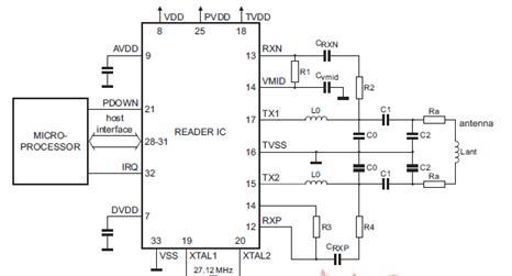
图3.CLRC663典型天线应用框图
CLEV663无接触读卡器评估板
This application note gives a detailed overview of the hardware for working with the RC663 contactless reader - we use the LPCXpresso LPC1769 and the Blueboard – the installation procedures of the Development Environment and the handling of the reader projects using the NFC Reader Library.
The demo reader is made up of 2 separate boards:
• A CLEV663B demo board (called Blueboard) provided by NXP. This is the primary platform for the RC663 reader chip and the current version is Blueboard v3.0 (see Fig 1). This board has connectors which are designed to exactly fit the ones of the companion, the LPCXpresso LPC 1769 development board.
• A commercial LPCXpresso LPC 1769 development board (12NC: 935291912598, Type: OM13000+598) which can be provided by NXP or bought directly on the market. See Ref. [10]. All projects can be used with the LPCXpresso LPC11U68 development board (12NC: 935303579598) as well.
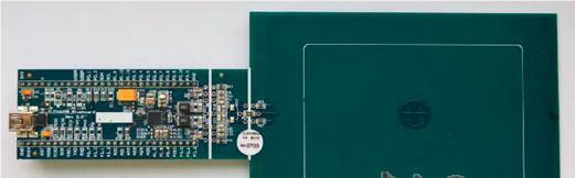
图4.CLEV663无接触读卡器评估板外形图
The RC663 demo board embeds the contactless communication transceiver IC RC663 with all its elements needed for transmission: EMC filter, matching network and the antenna. The RC663 supports different kind of contactless communication methods and protocols at 13.56 MHz:
• Reader/Writer mode supporting ISO/IEC14443A/MIFARE,
• Reader/Writer mode supporting ISO/IEC14443B,
• Reader/Writer mode supporting FeliCa scheme,
• Passive initiator mode according to NFCIP-1
• Reader/writer supporting ISO/IEC 15693,
• Reader/writer supporting ISO/IEC 18000-3 Mode 3,
• Refer to the data sheet of this IC [2] for more details
To work with the provided projects, one will also need an LPCXpresso LPC development board. Such a board is not included in the Blueboard hardware package.
The LPCXpresso LPC1769 development board integrates an NXP ARM Cortex-M3 microcontroller LPC1769 with 512 Kbytes of Flash memory and 64 Kbytes of RAM. Among others it integrates the following peripherals:
• Serial UART interface,
• SPI controller,
• I2C controller,
• Serial Wire test/debug interface,
• For detailed information, see LPC1769 product site [3]
The LPCXpresso board contains a JTAG/ SWD debugger called the “LPC-Link” and a target MCU. LPC-Link is equipped with a 10-pin JTAG header and it seamlessly connects to the target via USB to the computer.

图5.LPCXpresso LPC1769开发板外形图
责任编辑:HanFeng
【免责声明】
1、本文内容、数据、图表等来源于网络引用或其他公开资料,版权归属原作者、原发表出处。若版权所有方对本文的引用持有异议,请联系拍明芯城(marketing@iczoom.com),本方将及时处理。
2、本文的引用仅供读者交流学习使用,不涉及商业目的。
3、本文内容仅代表作者观点,拍明芯城不对内容的准确性、可靠性或完整性提供明示或暗示的保证。读者阅读本文后做出的决定或行为,是基于自主意愿和独立判断做出的,请读者明确相关结果。
4、如需转载本方拥有版权的文章,请联系拍明芯城(marketing@iczoom.com)注明“转载原因”。未经允许私自转载拍明芯城将保留追究其法律责任的权利。
拍明芯城拥有对此声明的最终解释权。
相关资讯
:
基于MC33771主控芯片的新能源锂电池管理系统解决方案

AMIC110 32位Sitara ARM MCU开发方案

基于AMIC110多协议可编程工业通信处理器的32位Sitara ARM MCU开发方案

基于展讯SC9820超低成本LTE芯片平台的儿童智能手表解决方案

基于TI公司的AM437x双照相机参考设计

基于MTK6580芯片的W2智能手表解决方案


 2012- 2022 拍明芯城ICZOOM.com 版权所有 客服热线:400-693-8369 (9:00-18:00)


