


 产品分类
产品分类
LPC210X之外部中断寄存器
 391
391
 拍明
拍明
LPC2101/LPC2102/LPC2103最多包含了三个外部中断输入作为可选择的管脚功能。管脚进行组合后,外部事件可以处理成三个独立的中断信号。外部中断输入能够可选择的用于将处理器从低功耗模式下唤醒。
此外,10个捕获输入没有可选择的将器件从低功耗模式唤醒功能,但也能够被用于外部中断。
Register descripTIon
有四个寄存器涉及外部中断

External Interrupt Flag register (EXTINT - 0xE01F C140)
外部中断标志寄存器
位
信号
描述
复位值
0
EINT0
对应管脚外部中断到来时,该标志位置位。写1清除该位,如果该中断处于电平触发模式,那么电平触发期间该位不能清除。
0
1
EINT1
同EINT0
0
2
EINT2
同EINT0
0
7:3
保留
NA
Interrupt Wake-up register (INTWAKE - 0xE01F C144)
中断唤醒寄存器
位
信号
描述
复位值
0
EXTWAKE0
置1时,指明EINT0中断将把处理器从低功耗模式唤醒
0
1
EXTWAKE1
置1时,指明EINT1中断将把处理器从低功耗模式唤醒
0
2
EXTWAKE2
置1时,指明EINT2中断将把处理器从低功耗模式唤醒
0
14:3
保留
NA
15
RTCWAKE
置1时,指明RTC中断将把处理器从低功耗模式唤醒
External Interrupt Mode register (EXTMODE - 0xE01F C148)
外部中断模式寄存器
位
信号
描述
复位值
0
EXTMODE0
0——EINT0电平触发
1——EINT0边沿触发
0
1
EXTMODE1
0——EINT1电平触发
1——EINT1边沿触发
0
2
EXTMODE2
0——EINT2电平触发
1——EINT2边沿触发
0
7:3
保留
NA
External Interrupt Polarity register (EXTPOLAR - 0xE01F C14C)
外部中断极性寄存器
位
信号
描述
复位值
0
EXTPOLAR0
0——EINT0低电平或者上升沿触发
1——EINT0高电平后者下降沿触发
0
1
EXTPOLAR1
0——EINT1低电平或者上升沿触发
1——EINT1高电平后者下降沿触发
0
2
EXTPOLAR2
0——EINT2低电平或者上升沿触发
1——EINT2高电平后者下降沿触发
0
7:3
保留
NA
【LPC2103】
LPC2103 是16/32 位ARM7TDMI-S CPU 微控制器,它内部带有32KB 的高速Flash存储器,128 位宽度的存储器接口和独特的加速结构,因此能够在最大时钟速率下运行32 位代码。
LPC2103适用于访回控制器和POS机等小型应用系统,具有较小的封装和极低的功耗;由于它内置了宽范围的串行通信接口(2 个UARTSPI.SSP和2个IC)和8KB的片内SRAM,因此在通信网关和协议转换器中也可采用LPC2103 作为主控芯片。由于其具有32/16 位定时器,增强型10 位ADC,定时器输出匹配PWM 特性,多达13 个边沿、电平触发的外部中断,32 条高速GPIO,使得LPC2103 微控制器特别适用于工业控制。
特点
※ 16-bit/32-bit ARM7TDMI-S微控制器在一个小LQFP48 包装.
※ 8 kB的片内静态RAM和32 kB片上闪存程序内存. 128-bit宽度接口/加速器可实现高速70 MHz操作.
※ ISP/IAP通过片内引导程序软件.单个Flash扇区或整片擦除100 ms和256字节编程1 ms.
※ 嵌入式ICE RT提供实时与片内RealMonitor软件调试.
※ 该10-bit的A / D转换器提供8个模拟输入转换时间,低至2.44µs。每通道和专用的结果寄存器,以尽量减少中断开销.
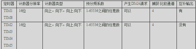
※ Two 32-bit定时器/联合七捕获外部事件计数器和七比较通道.
※ Two 16-bit定时器/ 3路捕获外部事件计数器和七比较通道.
※ 低功耗实时时钟(RTC)具有独立的电源和专用32千赫时钟输入.
※ 多个串行接口,包括两个UART (16C550),两个快速I2C(400 kbit / s)与缓冲和可变数据长度功能,SPI和SSP
※ 向量中断控制器,configurable优先级和向量地址.
※ 最多至32个5 V宽容快速通用I / O的pins.
※ 13边沿或电平触发的外部中断pins可用.
※ 70 MHz最大CPU时钟从可编程片上PLL可以以到10的MHz 25 MHz可能的输入频率和100µs建立时间
※ 片内集成振荡器与经营范围中的一个外部晶体从1 MHz到25 MHz.
※ 节电模式包括空闲模式,掉电与RTC主动模式,并掉电模式.
※ 单独使能/禁止外围功能以及周边时钟缩放额外的功率优化.
※ 处理器唤醒掉电模式,通过外部中断或RTC
框图
芯片内部结构框图:

【LPC2102】
The LPC2102 microcontrollers are based on a 16-bit/32-bit ARM7TDMI-S CPU with real-time emulation that combines the microcontroller with 16 kB of embedded high-speed flash memory. A 128-bit wide memory interface and a unique accelerator architecture enable 32-bit code execution at the maximum clock rate. For critical performance in interrupt service routines and DSP algorithms, this increases performance up to 30 pct over Thumb mode. For critical code size applications, the alternative 16-bit Thumb mode reduces code by more than 30 pct with minimal performance penalty.
Due to their tiny size and low power consumption, the LPC2102 are ideal for applications where miniaturization is a key requirement. A blend of serial communications interfaces ranging from multiple UARTs, SPI to SSP and two I2C-buses, combined with on-chip SRAM of 4 kB, make the LPC2102 very well suited for communication gateways and protocol converters. The superior performance also makes the LPC2102 suitable for use as math coprocessors. Various 32-bit and 16-bit timers, an improved 10-bit ADC, PWM features through output match on all timers, and 32 fast GPIO lines with up to nine edge or level sensitive external interrupt pins make the LPC2102 particularly suitable for industrial control and medical systems.

【LPC2101】
The LPC2101 microcontrollers are based on a 16-bit/32-bit ARM7TDMI-S CPU with real-time emulation that combines the microcontroller with 8 kB of embedded high-speed flash memory. A 128-bit wide memory interface and a unique accelerator architecture enable 32-bit code execution at the maximum clock rate. For critical performance in interrupt service routines and DSP algorithms, this increases performance up to 30 pct over Thumb mode. For critical code size applications, the alternative 16-bit Thumb mode reduces code by more than 30 pct with minimal performance penalty.
Due to their tiny size and low power consumption, the LPC2101 are ideal for applications where miniaturization is a key requirement. A blend of serial communications interfaces ranging from multiple UARTs, SPI to SSP and two I2C-buses, combined with on-chip SRAM of 2 kB, make the LPC2101 very well suited for communication gateways and protocol converters. The superior performance also makes the LPC2101 suitable for use as math coprocessors. Various 32-bit and 16-bit timers, an improved 10-bit ADC, PWM features through output match on all timers, and 32 fast GPIO lines with up to nine edge or level sensitive external interrupt pins make the LPC2101 particularly suitable for industrial control and medical systems.
责任编辑:Davia
【免责声明】
1、本文内容、数据、图表等来源于网络引用或其他公开资料,版权归属原作者、原发表出处。若版权所有方对本文的引用持有异议,请联系拍明芯城(marketing@iczoom.com),本方将及时处理。
2、本文的引用仅供读者交流学习使用,不涉及商业目的。
3、本文内容仅代表作者观点,拍明芯城不对内容的准确性、可靠性或完整性提供明示或暗示的保证。读者阅读本文后做出的决定或行为,是基于自主意愿和独立判断做出的,请读者明确相关结果。
4、如需转载本方拥有版权的文章,请联系拍明芯城(marketing@iczoom.com)注明“转载原因”。未经允许私自转载拍明芯城将保留追究其法律责任的权利。
拍明芯城拥有对此声明的最终解释权。
相关资讯
:
BAT剑指科大讯飞,能否让其重蹈Nuance覆辙?

三星在中国一面撤资,一面增资是为何?
半导体激光治疗仪是骗局吗?

2016全球十大电子元器件分销商排行榜

2016年10大全球电子元器件代理商排行一览表
STM32学习笔记:通用定时器基本定时功能


 2012- 2022 拍明芯城ICZOOM.com 版权所有 客服热线:400-693-8369 (9:00-18:00)


