


 产品分类
产品分类
基于Intel公司的Arria 10 SoC FPGA高性能低成本解决方案
 221
221
 拍明
拍明
原标题:基于Intel公司的Arria 10 SoC FPGA高性能低成本解决方案
Intel公司的Arria 10 SoC FPGA采用TSMC 20nm工艺技术,集成了双核ARM Cortex-A9MPCore硬件处理器系统(HPS)和业界一流可编逻辑技术诸如硬件浮点数字信号处理器(DSP)区块,提供具有丰富特性的嵌入外设,硬化浮点可变精度DSP区块,嵌入高速收发器,硬存储器控制器和协议IP控制器,CPU工作频率高达1.5GHz,主要用在无线基础设备,计算和存储设备,广播设备,军用设备和智能设备,有线100G线路卡,40G GPON,测试测量设备以及医疗图像诊断设备.本文介绍了Arria 10 SoC FPGA主要特性,框图以及Arria 10 SoC开发板主要特性,电源分布网络图和电路图.
The 20 nm ARM*-based Intel® Arria® 10 SoC delivers optimal performance, power efficiency, small form factor, and low cost for midrange applications. The Intel Arria 10 SoC, based on TSMC’s 20 nm process technology, combines a dual-core ARM Cortex*-A9 MPCore* Hard Processor System (HPS) with industry-leading programmable logic technology that includes hardened floating-point digital signal processing (DSP) blocks. The Intel Arria 10 SoC offers a processor with a rich feature set of embedded peripherals, hardened floating-point variable-precision DSP blocks, embedded high-speed transceivers, hard memory controllers, and protocol intellectual property (IP) controllers - all in a single highly integrated package.Intel Arria 10 SoCs: Higher System-Level Integration SoC in Production.
The Intel Arria 10 SoC combines architectural innovations with TSMC’s 20 nm process technology to deliver improvements in performance and power reduction:
65% higher processor performance with up to 1.5 GHz CPU operation per core†
60% higher performance versus the previous generation, over 500 MHz-capable FPGA logic core performance (15% higher performance than previous SoC)†
4X more transceiver bandwidth versus the previous generation (2X more bandwidth versus previous high-end FPGAs)†
4X higher system performance (2,400 Mbps DDR4 SDRAM, Hybrid Memory Cube support)†
More than 1,500 giga floating-point operation per second (GFLOPs) and up to 50 GFLOPs per Watt in a single device40% lower power with process technology improvement and innovative techniques for power reductionDesigned for Productivity
Design productivity is one of the driving philosophies of the Intel Arria 10 SoC architecture. The Intel Arria 10 SoC offers full software compatibility with previous generation SoC FPGAs, a broad ecosystem of ARM software and tools, and the enhanced FPGA and DSP hardware design flow.
Extensive ecosystem of ARM for software development.
Intel SoC FPGA Embedded Design Suite (SoC EDS) featuring the ARM* Development Studio 5* (DS-5*) Intel SoC FPGA Edition
Board support packages are available for popular operating system including Linux*, Wind River VxWorks, Wind River Linux, MicriumuC/OS-II and uC/OS-III, and more
Full software compatibility between 28 nm Cyclone® V SoC, Arria V SoC, and Intel Arria 10 SoC
Intel Quartus® Prime software FPGA design suite featuring:
High-level automated design flow with Open Computing Language (OpenCL™) compiler
Model-based digital signal processing (DSP) hardware design with DSP Builder for Intel FPGA
The Intel Arria 10 SoCs have been designed to meet the performance, power, and cost requirements for applications such as:
Wireless infrastructure equipment including remote radio unit and mobile backhaul
Compute and storage equipment including flash cache, cloud computing, and acceleration
Broadcast studio and distribution equipment including professional A/V and video conferencing
Military guidance, control, and intelligence equipment
Wireline 100G line cards, bridges and aggregation, 40G GPON
Test and measurement equipment
Diagnostic medical imaging equipment
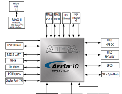
图1. Intel® Arria® 10 SoC框图
Arria 10 SoC开发板
The Arria 10 SoC development board provides a hardware platform for developing and prototyping lowpower,high-performance, and logic-intensive designs using Altera’s? Arria 10 SoC. The board provides awide range of peripherals and memory interfaces to facilitate the development of Arria 10 SoC designs.
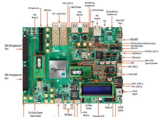
图2.Arria 10 SoC开发板外形图
Arria 10 SoC开发板主要特性:
• Arria 10 Soc (10AS066N3F40E2SG) in a 1517-pin FBGA (FineLine Ball-Grid Array) package
• FPGA configuration circuitry
• Active Serial (AS) x1 or x4 configuration (EPCQ1024L)
• MAX? V CPLD (5M2210ZF256) in a 256-pin FBGA package as the system controller
• MAX V CPLD (5M2210ZF256) in a 256-pin FBGA package as the I/O multiplier CPLD
• Clocking circuitry
• SI5338 programmable oscillator
• LMK04828 clock cleaner
• HPS clock options: 25 MHz, 33 MHz, and SMA input (2V5 LVCMOS)
• SI5112 100MHz clock generator for PCIe interface
• SI516 148.5 MHz voltage control oscillator for SDI interface
• Supported Memory
• HPS memory size (HILO card):
• 2GB DDR3 (256Mb x 40 x dual rank)
• 1GB DDR3 (256Mb x 40 x single rank)
• 1GB DDR4 (256Mb x 40 x single rank) - ships with kit
• FPGA memory size (HILO Card):
• 4GB DDR3 (256Mb x72 x dual rank)
• 2GB DDR3 (256Mb x72 x single rank)
• 2GB DDR4 (256Mb x 72 x single rank) - ships with kit
• 16MB QDRV (4Mb x 36)
• 128MB RLDRAM3(16Mb x 72)
• HPS Boot Flash (Flash card):
• NAND flash (x8) : 128MB (MT29F1G08ABBEAH4) - ships with kit
• QSPI flash: 128MB (MT25QU01GBBA8E12-0SIT) - ships with kit
• SD Micro flash card: 4GB (Kingston) - ships with kit
• Optional FPGA File Flash (Flash card):
• NAND flash (x8): 128MB (MT29F1G08ABBEAH4)
• QSPI flash: 128MB (MT25QU01GBBA8E12-0SIT)
• SD Micro flash card: 4GB (Kingston)
• Communication ports
• HPS Communication ports:
• USB 2.0 port (PHY PN: USB3320C-EZK)
• RGMII 10/100/1000 Ethernet port (PHY PN: KSZ9031RNXCA)
• USB-UART port (FT232R)
• DB-9 RS-232 Port (MAX3221)
• I2C port (I2C1 of shared I/O bit 12 and 13)
• FPGA I/O connections:
• FPGA V57.1 High Pin Count FMC slot
• FPGA Altera Low Pin Count FMC slot
• FMC_PCIe Gen2 x8 EP cable
• FPGA PCIe GEN1/2/3 x8 RC slot
• FPGA Communication ports:
• 2x SGMII Gigabit Ethernet ports (PHY PN: 88E1111-B2-NDC2C000)
• 2x 10Gb/s SFP+ ports
• Display port (DP)
• SDI/SDO video port
• SPI port
• UART port
• FPGA Debug ports:
• 16-bit Trace port (FPGA Trace)
• General user I/O
• LEDs and displays
• 4x FPGA user LEDs
• 4x HPS user LEDs
• Configuration load LED
• Configuration done LED
• Error LED
• 3x Configuration select LEDs
• 4x On-board USB-Blaster II status LEDs
• 2x FMC interface LEDs
• 2x UART data transmit and receive LEDs
• Power on LED
• Two-line character LCD display
• Push buttons
• CPU cold reset push button and one CPU warm reset push button
• Logic reset push button
• Program select push button
• Program configuration push button
• 4x FPGA user push buttons
• 4x HPS user push buttons
• External interrupt push button
• DIP Switches
• JTAG chain control DIP switch
• Board settings DIP switch
• FPGA configuration mode DIP switch
• General user DIP switch
• Power supply
• 12V DC Input
• Mechanical
• 7.175" x 9.3" rectangular form factor
责任编辑:Davia
【免责声明】
1、本文内容、数据、图表等来源于网络引用或其他公开资料,版权归属原作者、原发表出处。若版权所有方对本文的引用持有异议,请联系拍明芯城(marketing@iczoom.com),本方将及时处理。
2、本文的引用仅供读者交流学习使用,不涉及商业目的。
3、本文内容仅代表作者观点,拍明芯城不对内容的准确性、可靠性或完整性提供明示或暗示的保证。读者阅读本文后做出的决定或行为,是基于自主意愿和独立判断做出的,请读者明确相关结果。
4、如需转载本方拥有版权的文章,请联系拍明芯城(marketing@iczoom.com)注明“转载原因”。未经允许私自转载拍明芯城将保留追究其法律责任的权利。
拍明芯城拥有对此声明的最终解释权。
相关资讯
:
基于MC33771主控芯片的新能源锂电池管理系统解决方案

AMIC110 32位Sitara ARM MCU开发方案

基于AMIC110多协议可编程工业通信处理器的32位Sitara ARM MCU开发方案

基于展讯SC9820超低成本LTE芯片平台的儿童智能手表解决方案

基于TI公司的AM437x双照相机参考设计

基于MTK6580芯片的W2智能手表解决方案


 2012- 2022 拍明芯城ICZOOM.com 版权所有 客服热线:400-693-8369 (9:00-18:00)


