


 产品分类
产品分类
基于Renesas公司的RX65N和RX651系列RX MCU评估方案
 231
231
 拍明
拍明
原标题:Renesas RX65N和RX651系列RX MCU评估方案
Renesas公司的RX65N和RX651系列是采用32位RXv2核的新型主流RX微控制器,具有大容量RAM(高达2MB闪存和640KB SRAM),增强的安全性,连接性和人机接口HMI.工作频率120MHz,片上FPU,240 DMIPS,具有多种通信接口如以太网MAC,SD主接口,SD从接口,四SPI,CAN,12位ADC,RTC,加密功能,CMOS照相机接口,容性LCD控制器和2D绘图引擎.工作电压2.7- 3.6V,主要用在家用安全设备,家用计量设备,PC外设,建筑物管理,工业应用,有线连接,马达控制和人机接口等.本文介绍了RX65N和RX651系列主要特性,框图,以及RX65N Envision评估套件主要特性和指标,评估板主要元件分别图,电路图和材料清单.
RX65N and RX651 Groups are new mainstream RX microcontrollers with RXv2 core, large-capacity RAM, and enhanced security, connectivity, and HMI High Power Efficiency RXv2 core with maximum operating frequency of 120 MHz realizes high power efficiency of 34 CoreMark/mA, which enables battery life of endpoint devices, etc. to be maximized, as well as high performance.
Extensive communication functions and encryption functions realize secure updating of device control The RX65N Group and the RX651 Group can be divided into products having a code flash memory capacity of 1 MB or less, and or 1.5 MB or more. The products with 1 MB or less code flash memory is equipped with a large-capacity RAM of 256 KB for carrying out high-speed communication processing that is required for various communication interfaces such as Ethernet, USB, CAN, SD host/slave interface, and quad SPI. The products with 1.5 MB or more code flash memory have even more enhanced encryption functionality. Trusted secure IP protects encryption keys by controlling access. By combining this with a rich variety of communication functions high root-of-trust levels are achieved. Furthermore, protect and dual-bank functions that prevent erroneous writing of on-chip flash memory enable secure and easy program updating via a network. In addition, the large on-chip RAM of 640 KB allows high-speed processing of heavy loads, enabling rich user interfaces using the LCDC and 2D graphics engine.
Reduce development time The RX65N and RX651 Groups are highly compatible among the same series both in functional scalability and pin assignments. In addition, driver/middleware (FIT support), sample code-generation tools (code generators), and evaluation boards (starter kit and Envision Kit) are available, to allow reuse of most developed hardware/software resources. Partner tools that make it easy to build the kind of user interfaces (UI) that are essential for HMI are also available. All these enable seamless and scalable product development from small to large-scale applications easily and in a short time.
We offer the following solutions for reference for the RX651 Group and the RX65N Group to help you embed encryption technologies and HMI (human-machine interface) essential for IoT into your system immediately.
RX65N和RX651系列主要特性:
■ 32-bit RXv2 CPU core
• Max. operating frequency: 120 MHz
Capable of 240 DMIPS in operation at 120 MHz
• Single precision 32-bit IEEE-754 floating point
• Two types of multiply-and-accumulation unit (between memoriesand between registers)
• 32-bit multiplier (fastest instruction execution takes one CPU clockcycle)
• Divider (fastest instruction execution takes two CPU clock cycles)
• Fast interrupt
• CISC Harvard architecture with 5-stage pipeline
• Variable-length instructions: Ultra-compact code
• Supports the memory protection unit (MPU)
• JTAG and FINE (one-line) debugging interfaces
■ Low-power design and architecture
• Operation from a single 2.7- to 3.6-V supply
• Low power consumption: A product that supports all peripheralfunctions draws only 0.19 mA/MHz (Typ.).
• RTC is capable of operation from a dedicated power supply.
• Four low-power modes
■ On-chip code flash memory
• Supports versions with up to 2 Mbytes of ROM
• No wait cycles at up to 50 MHz or when the ROM cache is hit, onewaitstate at up to 100 MHz, two-wait state at above 100 MHz
• User code is programmable by on-board or off-board programming.
• Programming/erasing as background operations (BGOs)
• A dual-bank structure allows exchanging the start-up bank.
■ On-chip data flash memory
• 32 Kbytes, reprogrammable up to 100,000 times
• Programming/erasing as background operations (BGOs)
■ On-chip SRAM, no wait states
• 256K/640 Kbytes of SRAM (no wait states)
• 8 Kbytes of standby RAM (backup on deep software standby)
■ Data transfer
• DMACAa: 8 channels
• DTCb: 1 channel
• EXDMAC: 2 channels
• DMAC for the Ethernet controller: 1 channel
■ Reset and supply management
• Power-on reset (POR)
• Low voltage detection (LVD) with voltage settings
■ Clock functions
• External crystal resonator or internal PLL for operation at 8 to 24MHz
• Internal 240-kHz LOCO and HOCO selectable from 16, 18, and 20MHz
• 120-kHz clock for the IWDTa
■ Real-time clock
• Adjustment functions (30 seconds, leap year, and error)
• Real-time clock counting and binary counting modes are selectable
• Time capture function(for capturing times in response to event-signal input)
■ Independent watchdog timer
• 120-kHz (1/2 LOCO frequency) clock operation
■ Useful functions for IEC60730 compliance
• Oscillation-stoppage detection, frequency measurement, CRCA,IWDTa, self-diagnostic function for the A/D converter, etc.
• Register write protection function can protect values in importantregisters against overwriting.
■ Various communications interfaces
• Ethernet MAC (1 channel)
• PHY layer (1 channel) for host/function or OTG controller(1 channel) with full-speed USB 2.0 transfer
• CAN (compliant with ISO11898-1), incorporating 32 mailboxes (upto 2 channels)
• SCIg and SCIh with multiple functionalities (up to 11 channels)
Choose from among asynchronous mode, clock-synchronous mode,smart-card interface mode, simplified SPI, simplified I2C, andextended serial mode.
• SCIi with 16-byte transmission and reception FIFOs (up to 2channels)
• I2C bus interface for transfer at up to 1 Mbps (up to 3 channels)
• Four-wire QSPI (1 channel) in addition to RSPIc (3 channels)
• Parallel data capture unit (PDC) for the CMOS camera interface (notin 100-pin products)
• Graphic-LCD controller (GLCDC)
• 2D drawing engine (DRW2D)
• SD host interface (optional: 1 channel) with a 1- or 4-bit SD bus foruse with SD memory or SDIO
• SD slave interface (optional: 1 channel) with a 1- or 4-bit SD bus foruse with SD host interface
• MMCIF with 1-, 4-, or 8-bit transfer bus width
■ External address space
• Buses for full-speed data transfer (max. operating frequency of 60MHz)
• 8 CS areas
• 8-, 16-, or 32-bit bus space is selectable per area
• Independent SDRAM area (128 Mbytes)
■ Up to 25 extended-function timers
• 16-bit TPUa, MTU3a
• 8-bit TMRa (4 channels), 16-bit CMT (4 channels), 32-bit CMTW (2channels)
■ 12-bit A/D converter
• Two 12-bit units (8 channels for unit 0; 21 channels for unit 1)
• Self diagnosis, detection of analog input disconnection
■ 12-bit D/A converter: 2 channels
■ Temperature sensor for measuring temperaturewithin the chip
■ Encryption functions (optional)
• AES (key lengths: 128, 192, and 256 bits)
• Trusted Secure IP (TSIP)
■ Up to 136 pins for general I/O ports
• 5-V tolerance, open drain, input pull-up, switchable driving ability
■ Operating temp.range
• D-version: –40 ℃ to +85℃
• G-version: –40℃ to +105℃
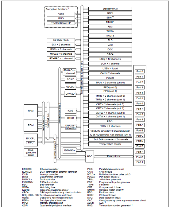
图1.RX65N和RX651系列框图
RX65N Envision评估套件
The Envision Kit allows quick and easy evaluation of the RX65N microcontrollers group, which is an excellent choice for your next low cost HMI (Human Machine Interface) project. Moreover the RX65N Envision Kit allows you to experience, through pre-installed demos, firmware updating using the new dual-bank flash function of the RX65N microcontroller, graphics performance using LCDC and a 2D drawing engine, and many more.
This manual is designed to describe the hardware features of the RX65N Envision Kit and is not intended as a comprehensive introduction to the RX65N microcontroller group, the e2 studio development IDE or the E2 Emulator Lite. Please refer to the relevant user manuals for more in-depth information.
RX65N Envision评估套件主要特性:
• In-circuit programming and debugging with E2 Lite On Board (E2OB).
• WQVGA (480 x 272) TFT LCD panel driven directly from the RX65N Graphic LCD Controller (GLCDC) peripheral.
• 23V LED driver circuit for LCD backlight.
• Graphics manipulation using the 2D Graphics Drawing Engine (DRW2D).
• Capacitive touch screen sampling via I2C controller.
• On-board QSPI serial Flash.
• USB 2.0 Host.
• Connection for external PmodTM based peripherals.
The RX65N Envision Kit board contains all the circuitry required for microcontroller operation. A variety of other peripherals are tracked into the RX65N Envision Kit PCB design, but not fitted as standard.
• Ethernet – Requires Ethernet RMII Phy IC and surface mount connector.
• SD Host Interface – Requires SDHI connector and power management IC.
• Joystick – Providing switch inputs for left, right, up, down and centre mapping to RX65N IRQ ports.
• Provision to expand functionality with ArduinoTM style shields.
RX65N Envision评估板主要指标:
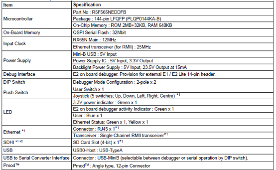
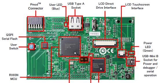
图2.RX65N Envision评估板元件布局图(1)
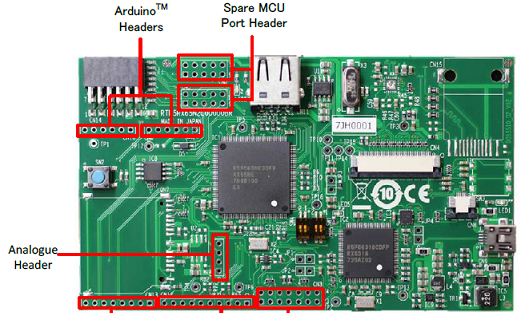
图3.RX65N Envision评估板元件布局图(2):底层
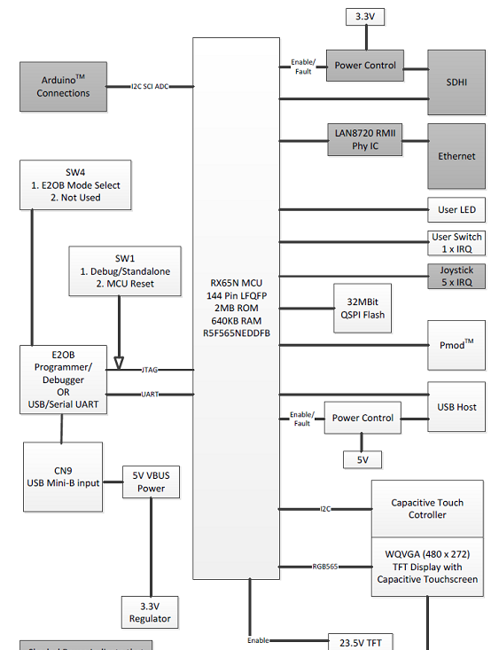
图.RX65N Envision评估板内部框图
RX65N Envision Kit Schematic
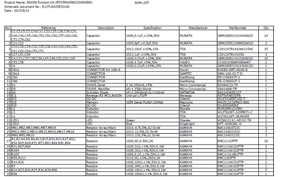
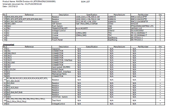
RX65N Envision评估板材料清单:
责任编辑:Davia
【免责声明】
1、本文内容、数据、图表等来源于网络引用或其他公开资料,版权归属原作者、原发表出处。若版权所有方对本文的引用持有异议,请联系拍明芯城(marketing@iczoom.com),本方将及时处理。
2、本文的引用仅供读者交流学习使用,不涉及商业目的。
3、本文内容仅代表作者观点,拍明芯城不对内容的准确性、可靠性或完整性提供明示或暗示的保证。读者阅读本文后做出的决定或行为,是基于自主意愿和独立判断做出的,请读者明确相关结果。
4、如需转载本方拥有版权的文章,请联系拍明芯城(marketing@iczoom.com)注明“转载原因”。未经允许私自转载拍明芯城将保留追究其法律责任的权利。
拍明芯城拥有对此声明的最终解释权。
相关资讯
:
基于MC33771主控芯片的新能源锂电池管理系统解决方案

AMIC110 32位Sitara ARM MCU开发方案

基于AMIC110多协议可编程工业通信处理器的32位Sitara ARM MCU开发方案

基于展讯SC9820超低成本LTE芯片平台的儿童智能手表解决方案

基于TI公司的AM437x双照相机参考设计

基于MTK6580芯片的W2智能手表解决方案


 2012- 2022 拍明芯城ICZOOM.com 版权所有 客服热线:400-693-8369 (9:00-18:00)


