


 产品分类
产品分类
ADI ADRF6650带DVGA和PLL/VCO的双下变换解决方案
 136
136
 拍明
拍明
原标题:ADI ADRF6650带DVGA和PLL/VCO的双下变换解决方案
ADI公司的ADRF6650是高度集成的下变换器,集成了两个混合器,两个数字开关衰减器,两个数字可变增益放大器,一个锁相环(PLL)和压控振荡器(VCO).此外还集成了两个RF平衡转换器(Balun),串行增益控制(SGC),用于时分复用(TDD)工作的快速使能输入.片上的RF平衡转换器使ADRF6650支持50 Ω终端RF输入.集成的无源混合器提供高度线性下变换器,用于200MHz滑动中频(IF)窗口.ADRF6650采用宽带方波限幅振荡器(LO)放大器,以达到450 MHz 到 2700 MHz的RF带宽.和通常的窄带正弦波LO放大器解决方案不同,该放大器允许LO可在极宽带宽上应用在高于或低下RF输入频率.集成的PLL/VCD使得连续LO 的频率范围从450 MHz 到 2900 MHz. PLL基准输入支持宽频率范围和包括集成相频检测器(PFD)前的基准分频器.ADRF6650采用先进的硅锗(SiGe)双极互补金属氧化物半导体(BiCMOS)工艺,56引脚RoHS兼容性8 mm × 8 mm LFCSP封装,工作温度−40℃ 到 +105℃.主要用在多波段/多标准蜂窝基站分集接收器,宽带无线连接分集式下变换器,多模式蜂窝扩展器和微微蜂窝基站.本文介绍了ADRF6650主要特性,功能框图,PLL/VCO框图,基本连接框图以及评估板ADRF6650-EVALZ主要特性,测试建立图,电路图,材料清单和PCB设计图.
The ADRF6650 is a highly integrated downconverter that integrates dual mixers, dual digital switched attenuators, dual digital variable gain amplifiers, a phase-locked loop (PLL), and voltage controlled oscillators (VCOs). In addition, the ADRF6650 integrates two radio frequency (RF) baluns, serial gain control (SGC) controls, and fast enable inputs for time division duplex (TDD) operation.
The on-chip RF baluns enable the ADRF6650 to support 50 Ω terminated RF inputs. The integrated passive mixer provides a highly linear downconversion for a 200 MHz, sliding, intermediate frequency (IF) window. The ADRF6650 uses broadband square wave limiting local oscillator (LO) amplifiers to achieve an RF bandwidth of 450 MHz to 2700 MHz. Unlike conventional narrow-band sine wave LO amplifier solutions, this amplifier permits the LO to be applied either above or below the RF input over an extremely wide bandwidth.
The ADRF6650 offers two alternatives for generating the differ-ential LO input signal: internally via the on-chip fractional-N synthesizer with low phase noise VCOs, or externally via a low phase noise LO signal. The integrated PLL/VCO enables contin-uous LO coverage from 450 MHz to 2900 MHz. The PLL reference input supports a wide frequency range and includes integrated reference dividers before the phase frequency detector (PFD).
The ADRF6650 is fabricated using an advanced silicon-germa-nium (SiGe) bipolar complementary metal-oxide semiconductor (BiCMOS) process. It is available in a 56-lead, RoHS-compliant, 8 mm × 8 mm, lead frame chip scale package (LFCSP) package with an exposed pad. Performance is specified over the −40℃to +105℃ maximum paddle temperature.
ADRF6650主要特性:
Dual down-converter with integrated fractional-N PLL/VCO
RF: 450 MHz to 2700 MHz continuous
LO frequency: 450 MHz to 2900 MHz, high-side or low-side injection
43 dB gain control range
Gain control with up/down and SPI
Integrated RF balun for single-ended 50 Ω inputs
Power supply: 3.3 and 5 V
8 mm × 8 mm, 56-lead LFCSP package
ADRF6650应用:
Multiband/multistandard cellular base station diversity receivers
Wideband radio link diversity downconverters
Multimode cellular extenders and picocells
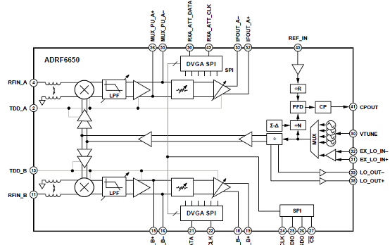
图1.ADRF6650功能框图
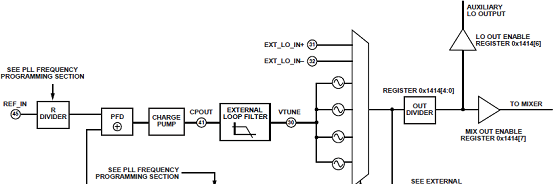
图2.PLL/VCO框图
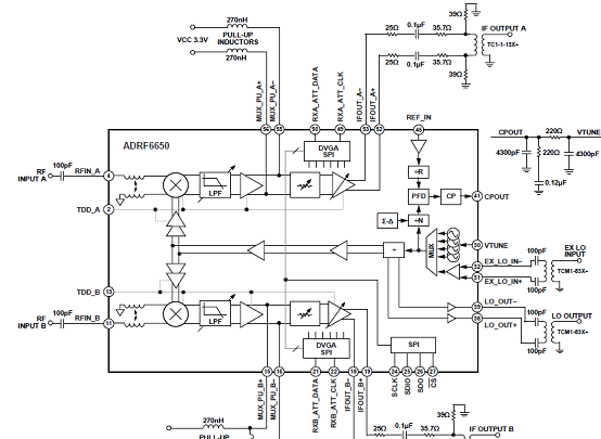
图3.ADRF6650基本连接框图
评估板ADRF6650-EVALZ
Evaluating the ADRF6650 450 MHz to 2700 MHz Dual Downconverter with DVGA and PLL/VCO
The ADRF6650-EVALZ is a 4-layer Rogers printed circuit board (PCB) and evaluates the performance of the ADRF6650. A photograph of the evaluation board is shown in Figure 1. The evaluation board contains the ADRF6650, a connector suited for a SDP-S controller board, power supply connectors, regulators, and subminiature Version A (SMA) connectors. The evaluation board requires an SDP-S controller board to allow software programming of the device.
The ADRF6650 is a high performance, dual downconverter that integrates mixers, digital switched attenuators, digital variable gain amplifiers (DVGAs), a phase-locked loop (PLL), and a voltage controlled oscillator (VCO). The device uses broadband, square wave limiting, local oscillator (LO) amplifiers to achieve an RF bandwidth of 450 MHz to 2700 MHz. Unlike conventional, narrow-band, sine wave LO amplifier solutions, the ADRF6650 allows the application of the LO either above or below the RF input, over a bandwidth of 450 MHz to 2900 MHz.
This user guide describes the ADRF6650-EVALZ evaluation board and software. For full details, see the ADRF6650 data sheet, which must be consulted in conjunction with this user guide when using the evaluation board.
评估板ADRF6650-EVALZ主要特性:
Full featured evaluation board for the ADRF6650
Single supply: 5.6 V (1 A capability required)
ACE software for control
EVALUATION KIT CONTENTS
ADRF6650-EVALZ evaluation board
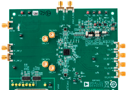
图4.评估板ADRF6650-EVALZ外形图

图5.评估板ADRF6650-EVALZ测试建立图

图6.评估板ADRF6650-EVALZ电路图(1)
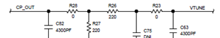
图7.PLL滤波器电路图
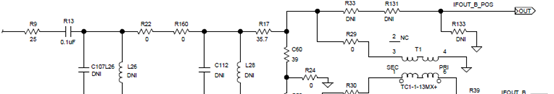
图8. IF输出电路图
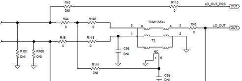
图9.LO输出电路图
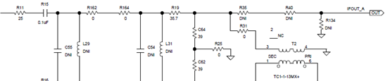
图10.外部LO输入电路图
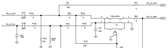
图11.ADRF6650 PLL电路图

图12.PLL/VCO电源电路
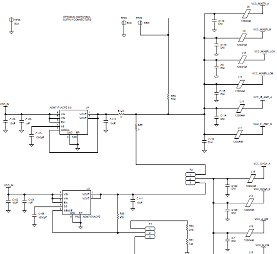
图13.RF/IF电源电路
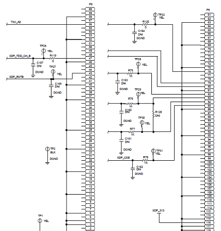
图14.SDP-S连接器电路
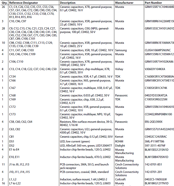
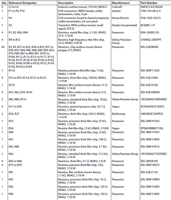
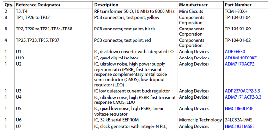
评估板ADRF6650-EVALZ材料清单:
责任编辑:David
【免责声明】
1、本文内容、数据、图表等来源于网络引用或其他公开资料,版权归属原作者、原发表出处。若版权所有方对本文的引用持有异议,请联系拍明芯城(marketing@iczoom.com),本方将及时处理。
2、本文的引用仅供读者交流学习使用,不涉及商业目的。
3、本文内容仅代表作者观点,拍明芯城不对内容的准确性、可靠性或完整性提供明示或暗示的保证。读者阅读本文后做出的决定或行为,是基于自主意愿和独立判断做出的,请读者明确相关结果。
4、如需转载本方拥有版权的文章,请联系拍明芯城(marketing@iczoom.com)注明“转载原因”。未经允许私自转载拍明芯城将保留追究其法律责任的权利。
拍明芯城拥有对此声明的最终解释权。
相关资讯
:
基于MC33771主控芯片的新能源锂电池管理系统解决方案

AMIC110 32位Sitara ARM MCU开发方案

基于AMIC110多协议可编程工业通信处理器的32位Sitara ARM MCU开发方案

基于展讯SC9820超低成本LTE芯片平台的儿童智能手表解决方案

基于TI公司的AM437x双照相机参考设计

基于MTK6580芯片的W2智能手表解决方案


 2012- 2022 拍明芯城ICZOOM.com 版权所有 客服热线:400-693-8369 (9:00-18:00)


