Renesas RX65N系列云通信性能评估方案
 102
102
 拍明
拍明
原标题:Renesas RX65N系列云通信性能评估方案
Renesas公司的RX65N云套件是一种采用RX65N微控制器的云通信性能评估套件, 可以通过 Wi-Fi 连接到 Amazon Web Services (AWS),为开发人员提供一个理想的评估环境,支持用户启动物联网设备的开发.该套件包括一个 Wi-Fi 通信模块,一个温度/湿度传感器,一个光传感器,一个 3 轴加速度计,一个用于串行通信的 USB 端口和一个用于调试的 USB 端口.该套件中所使用的 RX65N 微控制器是新一代通用 mcu,带有人机界面 (HMI) 和非常适用于物联网边缘设备的安全功能.借助内置的双组功能和值得信赖的安全 IP 功能,您就能够建立安全的云通信,并能够轻松安全地进行固件更新.具有实现 AWS 云的安全连接, 通过 Amazon FreeRTOS认证,辅助物联网设备的原型开发,免费提供可编辑,可调试的 AWS 通信示例程序,提供应用指南,帮助用户理解示例程序的运行,从而减少实际的产品开发工时,可以轻松将一般必需的物联网功能编译到设备中.本文介绍了RX65N系列主要特性, 系列框图以及Renesas RX65N云套件主要特性和电路图与PCB设计图.
120-MHz 32-bit RX MCU, on-chip FPU, 240 DMIPS, up to 2-MB flash memory(supportive of the dual bank function), 640-KB SRAM, various communications interfaces including Ethernet MAC, SD host interface (optional), SD slave interface (optional), quad SPI, and CAN, 12-bit A/D converter, RTC,Encryption functions (optional), CMOS camera interface, Graphic-LCD controller, 2D drawing engine
RX65N系列主要特性:
■ 32-bit RXv2 CPU core
Max.operating frequency: 120 MHzCapable of 240 DMIPS in operation at 120 MHz
Single precision 32-bit IEEE-754 floating point
Two types of multiply-and-accumulation unit (between memoriesand between registers)
32-bit multiplier (fastest instruction execution takes one CPU clockcycle)
Divider (fastest instruction execution takes two CPU clock cycles)
Fast interrupt
CISC Harvard architecture with 5-stage pipeline
Variable-length instructions: Ultra-compact code
Supports the memory protection unit (MPU)
JTAG and FINE (one-line) debugging interfaces
■ Low-power design and architecture
Operation from a single 2.7- to 3.6-V supply
Low power consumption: A product that supports all peripheralfunctions draws only 0.19 mA/MHz (Typ.).
RTC is capable of operation from a dedicated power supply.
Four low-power modes
■ On-chip code flash memory
Supports versions with up to 2 Mbytes of ROM
No wait cycles at up to 50 MHz or when the ROM cache is hit, onewaitstate at up to 100 MHz, two-wait state at above 100 MHz
User code is programmable by on-board or off-board programming.
Programming/erasing as background operations (BGOs)
A dual-bank structure allows exchanging the start-up bank.
■ On-chip data flash memory
32 Kbytes, reprogrammable up to 100,000 times
Programming/erasing as background operations (BGOs)
■ On-chip SRAM, no wait states
256K/640 Kbytes of SRAM (no wait states)
8 Kbytes of standby RAM (backup on deep software standby)
■ Data transfer
DMACAa: 8 channels
DTCb: 1 channel
EXDMAC: 2 channels
DMAC for the Ethernet controller: 1 channel
■ Reset and supply management
Power-on reset (POR)
Low voltage detection (LVD) with voltage settings
■ Clock functions
External crystal resonator or internal PLL for operation at 8 to 24MHz
Internal 240-kHz LOCO and HOCO selectable from 16, 18, and 20MHz
120-kHz clock for the IWDTa
■ Real-time clock
Adjustment functions (30 seconds, leap year, and error)
Real-time clock counting and binary counting modes are selectable
Time capture function(for capturing times in response to event-signal input)
■ Independent watchdog timer
120-kHz (1/2 LOCO frequency) clock operation
■ Useful functions for IEC60730 compliance
Oscillation-stoppage detection, frequency measurement, CRCA,IWDTa, self-diagnostic function for the A/D converter, etc.
Register write protection function can protect values in importantregisters against overwriting.
■ Various communications interfaces
Ethernet MAC (1 channel)
PHY layer (1 channel) for host/function or OTG controller(1 channel) with full-speed USB 2.0 transfer
CAN (compliant with ISO11898-1), incorporating 32 mailboxes (upto 2 channels)
SCIg and SCIh with multiple functionalities (up to 11 channels)
Choose from among asynchronous mode, clock-synchronous mode,smart-card interface mode, simplified SPI, simplified I2C, andextended serial mode.
SCIi with 16-byte transmission and reception FIFOs (up to 2channels)
I2C bus interface for transfer at up to 1 Mbps (up to 3 channels)
Four-wire QSPI (1 channel) in addition to RSPIc (3 channels)
Parallel data capture unit (PDC) for the CMOS camera interface
Graphic-LCD controller (GLCDC)
2D drawing engine (DRW2D)
SD host interface (optional: 1 channel) with a 1-or 4-bit SD bus foruse with SD memory or SDIO
SD slave interface (optional: 1 channel) with a 1-or 4-bit SD bus foruse with SD host interface
MMCIF with 1-, 4-, or 8-bit transfer bus width
■ External address space
Buses for full-speed data transfer (max. operating frequency of 60MHz)
8 CS areas
8-, 16-, or 32-bit bus space is selectable per area
Independent SDRAM area (128 Mbytes)
■ Up to 25 extended-function timers
16-bit TPUa, MTU3a
8-bit TMRa (4 channels), 16-bit CMT (4 channels), 32-bit CMTW (2channels)
■ 12-bit A/D converter
Two 12-bit units (8 channels for unit 0; 21 channels for unit 1)
Self diagnosis, detection of analog input disconnection
■ 12-bit D/A converter: 2 channels
■ Temperature sensor for measuring temperaturewithin the chip
■ Encryption functions (optional)
AES (key lengths: 128, 192, and 256 bits)
Trusted Secure IP (TSIP)
■ Up to 136 pins for general I/O ports
5-V tolerance, open drain, input pull-up, switchable driving ability
■ Operating temp.range
D-version: –40 C to +85 C
G-version: –40 C to +105 C
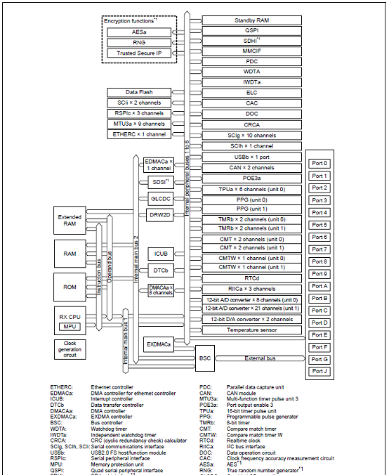
图1.RX65N系列框图
Renesas RX65N云套件
The Renesas RX65N Cloud Kit is a cloud communication performance evaluation kit that uses the RX65N microcontroller and can connect via Wi-Fi to Amazon Web Services (AWS). It provides an ideal evaluation environment for developers and supports the start of IoT device development by users.
The kit includes a Wi-Fi communication module, a temperature/humidity sensor, an optical sensor, a 3-axis accelerometer, a USB port for serial communications, and another USB port for debugging. The sensor and other data that is uploaded from the kit to AWS can be observed in the dashboard. The program can also be edited or debugged in Renesas’e2 studio Integrated Development Environment (IDE), by connecting the kit to a PC.
The RX65N microcontroller used in this kit is the next-generation general-purpose MCU, with Human Machine Interface (HMI) and security features that are ideal for IoT Edge devices. The built-in dual-bank functionality and Trusted Secure IP features will allow you to establish secure cloud communications and conduct firmware updates, both easily and securely.
Renesas RX65N云套件主要特性:
Allows for safe and secure connection to the AWS cloud
The combination of the Renesas RX65N Cloud Kit and Amazon FreeRTOS is Amazon FreeRTOS certified
Assists in IoT device prototyping
Editable and debuggable AWS Communications sample programs provided free of charge
Application notes available for understanding the behavior of the sample programs
Reduces actual product development man hours
The sample program is Amazon FreeRTOS-based; take advantage of the vast ecosystem of existing tools developed for the FreeRTOS kernel
The software library is already available within Amazon FreeRTOS which means you can easily program generally necessary IoT features into your devices
Two Types of Programs for Evaluating Cloud Communications
Basic AWS communications program
Sends a "Hello World" text message to the AWS cloud at regular intervals
Amazon FreeRTOS certified
Communicates wirelessly using Wi-Fi
Program for uploading sensor and other data to the AWS cloud, and for observing the information in the dashboard
Sends data from its three on-board sensors to the AWS cloud at regular intervals
Allows for observation of the sensor data in the dashboard
The Cloud Option Board connects to an RX Target Board to enable internet services via WiFi. It also provides a variety of environmental sensors for data measurement and logging purposes. The design is also easily extendable with a variety of measurement and communications options available.
This manual describes the technical details of the hardware that is included in the Cloud Option Board. It also describes the connectivity of the Cloud Option Board to the RX Target Board and the PmodTMWiFi module.
云选项板主要特性:
The Cloud Option Board extends an RX Target Board with the following additional features:
• PmodTM Connection for WiFi module (or other PmodTM peripherals).
• Additional storage via QSPI Serial Flash memory.
• Data acquisition from ambient light, Environmental (Pressure, humidity, temperature, gas) and Inertial Sensors.
• USB Serial Connection.
• USB Function connection.
• GroveTM connectors to allow off-board connectivity of Serial, I2C and analogue.
• Re-sited Reset and User Switches.
• Power Indicating LED and two User-controllable LEDs

图2. 云选项板,RX65N目标板和SilexPmod模块外形图
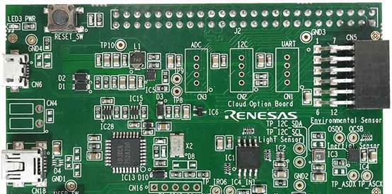
图3. 云选项板外形图
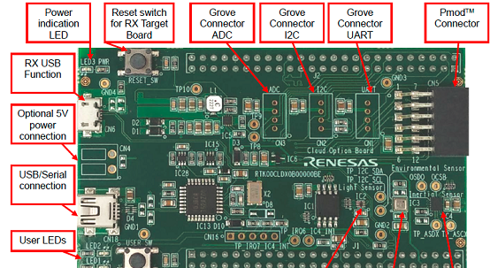
图4. 云选项板顶层概述图
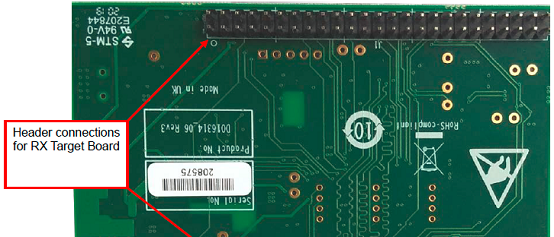
图5. 云选项板底层概述图
责任编辑:David
【免责声明】
1、本文内容、数据、图表等来源于网络引用或其他公开资料,版权归属原作者、原发表出处。若版权所有方对本文的引用持有异议,请联系拍明芯城(marketing@iczoom.com),本方将及时处理。
2、本文的引用仅供读者交流学习使用,不涉及商业目的。
3、本文内容仅代表作者观点,拍明芯城不对内容的准确性、可靠性或完整性提供明示或暗示的保证。读者阅读本文后做出的决定或行为,是基于自主意愿和独立判断做出的,请读者明确相关结果。
4、如需转载本方拥有版权的文章,请联系拍明芯城(marketing@iczoom.com)注明“转载原因”。未经允许私自转载拍明芯城将保留追究其法律责任的权利。
拍明芯城拥有对此声明的最终解释权。


 产品分类
产品分类




 2012- 2022 拍明芯城ICZOOM.com 版权所有 客服热线:400-693-8369 (9:00-18:00)


