


 产品分类
产品分类
Cypress CY8C38系列怀孕监视器PSoC开发方案
 132
132
 拍明
拍明
原标题:Cypress CY8C38系列怀孕监视器PSoC开发方案
怀孕监视器采用监测荷尔蒙水平来实现, 荷尔蒙水平监测由三种标准方法:尿液, 唾液和体温.每种检测需要模拟前端来实现.本文介绍了采用Cypress公司的CY8C38系列来开发怀孕监视器的确具体方案,方框图以及CY8C38 系列特性,框图,CY8C38系列典型应用电路图以及CY8CKIT-001 PSoC开发板主要特性,电路图和材料清单.
Fertility Monitors are devices that monitor fertility levels by monitoring hormone levels. A fertility monitor may analyze hormone levels in bodily fluids, resistance in bodily fluids, basal temperature, or a combination of these methods. There are three standard methods for monitoring hormone levels:
Urine: Tests for luteinizing hormone surge
Saliva: Detects changing electrolyte levels
Temperature: Monitors basal body temperature to predict cycles
Each of these sensing methods require an analog front end (AFE) to perform the necessary measurements. Fertility Monitors are battery powered devices so active power consumption and sleep current are important considerations. A fertility monitor also includes a display, memory for storage of fertility reading history, serial communication such as USB. A touchscreen or capsense user interface may also be seen in fertility monitors.
PSoC® 3 and PSoC 5 provide a scalable platform which provides all the requisite circuitry to provide a configurable Fertility Monitor on Chip, including:
• High precision Analog front end, including a 0.1% accurate Voltage reference and up to 20 bits of resolution
• Circuitry for sequencing and driving LED for optical measurement of the test strip and the circuitry for reading the photodiode to create a full optical measurement system
• LCD direct drive and control
• Low active and sleep mode power consumption, with full operation down to 0.5V
• CapSense fully integrated
• FS USB
• On chip EEPROM
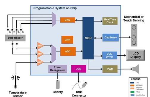
图1. 怀孕监视器框图
PSoC®3 具有独特的可配置模块阵列,是真正的系统级解决方案,能够通过单个芯片提供 MCU、存储器、模拟和数字外设功能。
CY8C38 系列提供了一种新型的信号采集、信号处理和控制方法,并具有高精度、高带宽和高灵活性等特点。其模拟功能涵盖了从热电偶信号(接近直流电压)到超声波信号的广泛信号范围。CY8C38 系列可以处理数十个数据采集通道以及每个 GPIO 引脚上的模拟输入。CY8C38 系列还是一个高性能的可配置数字系统,具有 USB、多主控 I2C 以及 CAN 等接口。除了通信接口之外,CY8C38 系列还具有易于配置的逻辑阵列,至所有 I/O 引脚的灵活路由,以及高性能的单周期 8051 微处理器内核。通过分层式电路图设计输入工具 PSoC® Creator™,设计人员可以使用包含众多预建组件和布尔基元的资料库,轻松创建系统级设计。使用 CY8C38 系列不仅可以实现模拟和数字材料表的集成,而且只需通过简单的固件更新,即可轻松纳入最新的设计变更。
CY8C38 系列特性:
单周期 8051 CPU 内核
工作频率介于 DC 至 67 MHz 之间
8x8 乘法和除法指令
闪速程序存储器,高达 64 KB,100,000 次写循环,20 年保留时间,多种安全特性
高达 8 KB 的 ECC 或配置闪存
高达 8 KB 的 SRAM 存储器
高达 2 KB 的 EEPROM 存储器,1M 次写循环,20 年保留时间
24 通道 DMA,多层 AHB 总线访问
• 可编程链式描述符和优先级
• 支持高带宽 32 位传输
低电压,超低功耗
宽广的工作电压范围:0.5V 至 5.5V
高效升压调节器(输入 0.5V,输出 1.8V-5.0V)
在 3 MHz 下为 0.8 mA,在 6 MHz 下为 1.2 mA,在 48 MHz下为 6.6 mA
低功耗模式包括:
• 1 μA 睡眠模式,提供实时时钟和欠压检测 (LVD) 中断
• 200 nA 休眠模式, RAM 保留数据
通用 I/O 系统
28 至 72 个 I/O (62 个 GPIO、8 个 SIO、2 个 USBIO[1])
可从任意 GPIO 路由至任意数字或模拟外设
任何 GPIO 都具有 LCD 直接驱动功能,能够驱动多达 46x16个段 (Segment)[1]
任何 GPIO 均提供 CapSense® 支持 [4]
1.2V 至 5.5V I/O 接口电压,多达 4 个电压域
任何引脚或端口都可设置成可接受独立的可屏蔽 IRQ
施密特触发器 TTL 输入
所有 GPIO 均可配置为开漏高电平/ 低电平、上拉/ 下拉、High-Z 或强输出
在加电复位 (POR) 时可配置 GPIO 引脚的状态
SIO 具有 25 mA 的灌电流能力
数字外设
20 至 24 个基于 PLD 的可编程通用数字模块
Full CAN 2.0b RX 缓冲区(16 个)和 TX 缓冲区(8 个)[1]
全速 (FS) USB 2.0 12 Mbps (采用内部振荡器) [1]
多达 4 个 16 位可配置定时器、计数器和 PWM 模块
标准外设库
• 8、16、24 和 32 位定时器、计数器和 PWM
• SPI、UART、I2C
• 目录中列出的许多其他外设
高级外设库
• 循环冗余校验 (Cyclic Redundancy Check, CRC)
• 伪随机序列 (Pseudo Random Sequence, PRS) 发生器
• LIN 总线 2.0
• 正交解码器
模拟外设 (1.71V ≤ Vdda ≤ 5.5V)
-40℃ 至 +85℃ 时内部电压参考为 1.024V±0.1% (14 ppm/℃)
具有 12 至 20 位分辨率的可配置 Delta-Sigma ADC
• 采样率高达 192 ksps
• 可编程增益级:x0.25 至 x16
• 12 位模式, 192 ksps, 70 dB SNR, 1 位 INL/DNL
• 16 位模式, 48 ksps, 90 dB SNR, 1 位 INL/DNL
67 MHz 24 位定点数字滤波器模块 (DFB),用于实现 FIR 和IIR 滤波器
多达四个 8 位 8 Msps IDAC 或 1 Msps VDAC
四个响应时间为 75 ns 的电压比较器
多达四个驱动能力为 25 mA 的未赋定运算放大器
多达四个可配置的多功能模拟模块。配置示例包括 PGA、TIA、混频器,以及采样和保持 (Sample and Hold)
CapSense 支持
编程、调试和跟踪
JTAG(4 线)接口,串行线调试 (Serial Wire Debug, SWD)(2 线)接口,以及单线浏览器 (Single Wire Viewer, SWV)接口
8 个地址断点和 1 个数据断点
4 KB 的指令跟踪缓冲区
支持通过 I2C、SPI、UART、USB 以及其他接口进行引导加载程序编程
高精度、可编程时钟
涵盖整个温度和电压范围的 3 至 62 MHz 内部振荡器
4 至 33 MHz 晶振,能够实现晶振 PPM 精度
内部 PLL 能够生成高达 67 MHz 的时钟
32.768 kHz 监视晶振
频率为 1 kHz、33 kHz 和 100 kHz 的低功耗内部振荡器
温度和封装
-40℃ 至 +85℃ 工业级温度
48 引脚 SSOP、48 引脚 QFN、68 引脚 QFN 以及 100 引脚TQFP 封装可供选择
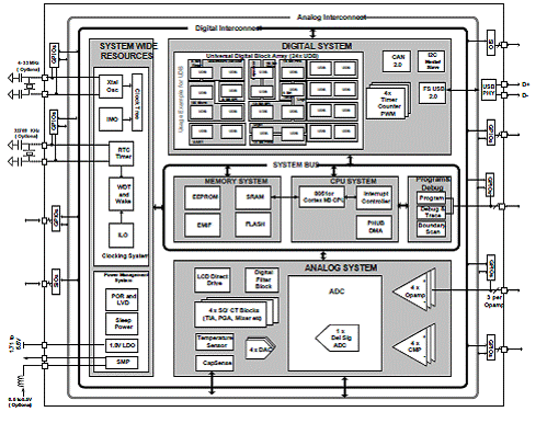
图2. CY8C38 系列简化的框图

图3. CY8C38 系列PSoC供电系统框图
CY8CKIT-001 PSoC开发板
The CY8CKIT-001 PSoC® Development Kit provides you a common development platform where you can prototype and evaluate different solutions using any one of the PSoC 1, PSoC 3, or PSoC 5 architectures. This guide and kit gives you a practical understanding of PSoC technology. In addition, the kit gives several example projects with step-by-step instructions to enable you to easily get started developing PSoC solutions. This kit includes PSoC CY8C28, CY8C38, and CY8C55 Family Processor Modules. The CY8CKIT-001 PSoC Development Kit supports projects across the PSoC 1, PSoC 3, and PSoC 5 architectures.
CY8CKIT-001 PSoC开发板包括:
The CY8CKIT-001 PSoC Development Kit includes:
■ PSoC Development Board
■ PSoC CY8C28 Family Processor Module
■ PSoC CY8C38 Family Processor Module
■ PSoC CY8C55 Family Processor Module
■ MiniProg3 Programmer and Debug tool
■ USB Cable
■ 12V Power Supply Adapter
■ Wire Pack
■ Printed Documentation
❐ Quick Start
❐ Schematic PSoC Development Board Design
■ Software CD for PSoC 1, which includes
❐ PSoC® Designer™ IDE
❐ PSoC® Programmer™ Software
❐ CY8C28 Data Sheets
❐ Kit Release Notes
❐ Software Release Notes
❐ Example Project Files, Firmware, And Documentation
■ Software CD for PSoC 3 / PSoC 5, which includes
❐ PSoC® Creator™ IDE
❐ PSoC Programmer Software
❐ CY8C38 Data Sheet
❐ CY8C55 Data Sheet
❐ Kit Release Notes
❐ Software Release Notes
❐ Example Project Files, Firmware, And Documentation
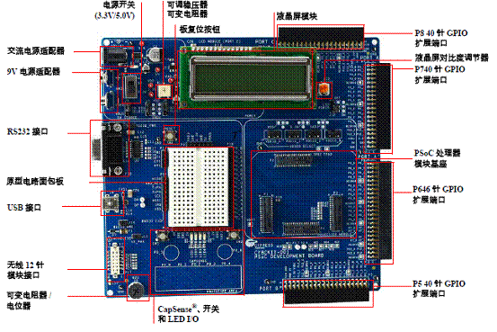
图5.CY8CKIT-001 PSoC开发板外形图
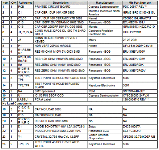
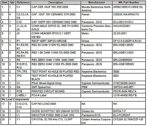
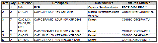
CY8CKIT-001 PSoC开发板材料清单:
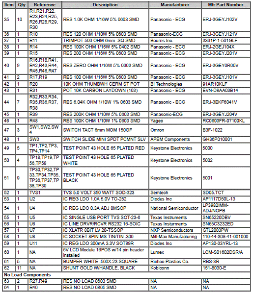
CY8C28处理器模块材料清单:
CY8C29处理器模块材料清单:
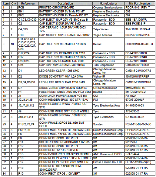
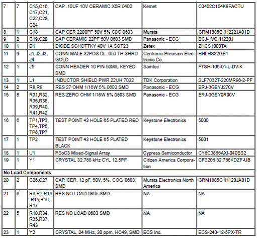
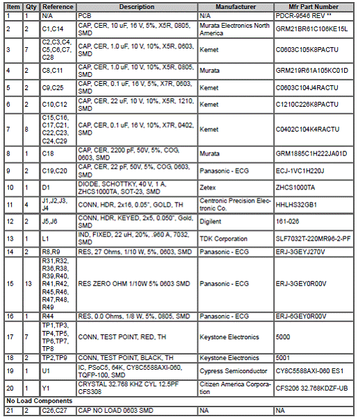
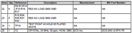
CY8C38处理器模块材料清单:
CY8C55处理器模块材料清单:
责任编辑:HanFeng
【免责声明】
1、本文内容、数据、图表等来源于网络引用或其他公开资料,版权归属原作者、原发表出处。若版权所有方对本文的引用持有异议,请联系拍明芯城(marketing@iczoom.com),本方将及时处理。
2、本文的引用仅供读者交流学习使用,不涉及商业目的。
3、本文内容仅代表作者观点,拍明芯城不对内容的准确性、可靠性或完整性提供明示或暗示的保证。读者阅读本文后做出的决定或行为,是基于自主意愿和独立判断做出的,请读者明确相关结果。
4、如需转载本方拥有版权的文章,请联系拍明芯城(marketing@iczoom.com)注明“转载原因”。未经允许私自转载拍明芯城将保留追究其法律责任的权利。
拍明芯城拥有对此声明的最终解释权。
相关资讯
:
基于MC33771主控芯片的新能源锂电池管理系统解决方案

AMIC110 32位Sitara ARM MCU开发方案

基于AMIC110多协议可编程工业通信处理器的32位Sitara ARM MCU开发方案

基于展讯SC9820超低成本LTE芯片平台的儿童智能手表解决方案

基于TI公司的AM437x双照相机参考设计

基于MTK6580芯片的W2智能手表解决方案


 2012- 2022 拍明芯城ICZOOM.com 版权所有 客服热线:400-693-8369 (9:00-18:00)


