


 产品分类
产品分类
Logic PD TI TMS320C6748开发方案
 116
116
 拍明
拍明
原标题:Logic PD TI TMS320C6748开发方案
Logic PD公司的Zoom™ OMAP-L138 EVM 开发套件包括应用基板和用户接口板,支持TI公司的OMAP-L138应用处理器和tms320C6748数字信号处理器(DSP), 主要用在医疗,工业设备,音频设备以及通信产品.本文介绍了TI 公司的TMS320C6748定点/浮点数字信号处理器(DSP)主要特性,方框图,以及Zoom™ OMAP-L138 EVM开发套件主要特性, 应用基板电路图和材料清单, 用户接口板电路图和材料清单.
The device is a low-power applications processor based on a C674x DSP core. It provides significantly lower power than other members of the TMS320C6000™ platform of DSPs.
The device enables OEMs and ODMs to quickly bring to market devices featuring robust operating systems support, rich user interfaces, and high processing performance life through the maximum flexibility of a fully integrated mixed processor solution.
The device DSP core uses a two-level cache-based architecture. The Level 1 program cache (L1P) is a 32KB direct mapped cache and the Level 1 data cache (L1D) is a 32KB 2-way set-associative cache. The Level 2 program cache (L2P) consists of a 256KB memory space that is shared between program and data space. L2 memory can be configured as mapped memory, cache, or combinations of the two.
Although the DSP L2 is accessible by other hosts in the system, an additional 128KB RAM shared memory is available for use by other hosts without affecting DSP performance.
For security enabled devices, TI’s Basic Secure Boot allows users to protect proprietary intellectual property and prevents external entities from modifying user-developed algorithms. By starting from a hardware-based “root-of-trust”, the secure boot flow guarantees a known good starting point for code execution. By default, the JTAG port is locked down to prevent emulation and debug attacks but can be enabled during the secure boot process during application development. The boot modules themselves are encrypted while sitting in external non-volatile memory, such as flash or EEPROM, and are decrypted and authenticated when loaded during secure boot. This protects customers’ IP and enables them to securely set up the system and begin device operation with known, trusted code. Basic Secure Boot utilizes either SHA-1 or SHA-256, and AES-128 for boot image validation. It also uses AES-128 for boot image encryption. The secure boot flow employs a multi-layer encryption scheme which not only protects the boot process but offers the ability to securely upgrade boot and application software code. A 128-bit device-specific cipher key, known only to the device and generated using a NIST-800-22 certified random number generator, is used to protect customer encryption keys. When an update is needed, the customer creates a new encrypted image using its encryption keys. Then the device can acquire the image via an external interface, such as Ethernet, and overwrite the existing code.
The peripheral set includes: a 10/100 Mb/s Ethernet MAC (EMAC) with a Management Data Input/Output (MDIO) module; one USB2.0 OTG interface; one USB1.1 OHCI interface; two inter-integrated circuit (I2C) Bus interfaces; one multichannel audio serial port (McASP) with 16 serializers and FIFO buffers; two multichannel buffered serial ports (McBSP) with FIFO buffers; two SPI interfaces with multiple chip selects; four 64-bit general-purpose timers each configurable (one configurable as watchdog); a configurable 16-bit host port interface (HPI) ; up to 9 banks of 16 pins of general-purpose input/output(GPIO) with programmable interrupt/event generation modes, multiplexed with other peripherals; three UART interfaces (each with RTS and CTS); two enhanced high-resolution pulse width modulator (eHRPWM) peripherals; 3 32-bit enhanced capture (eCAP) module peripherals which can be configured as 3 capture inputs or 3 auxiliary pulse width modulator (APWM) outputs; and 2 external memory interfaces: an asynchronous and SDRAM external memory interface (EMIFA) for slower memories or peripherals, and a higher speed DDR2/Mobile DDR controller.
The Ethernet Media Access Controller (EMAC) provides an efficient interface between the device and a network. The EMAC supports both 10Base-T and 100Base-TX, or 10 Mbits/second (Mbps) and 100 Mbps in either half- or full-duplex mode. Additionally an Management Data Input/Output (MDIO) interface is available for PHY configuration. The EMAC supports both MII and RMII interfaces.
The SATA controller provides a high-speed interface to mass data storage devices. The SATA controller supports both SATA I (1.5 Gbps) and SATA II (3.0 Gbps).
The Universal Parallel Port (uPP) provides a high-speed interface to many types of data converters, FPGAs or other parallel devices. The UPP supports programmable data widths between 8- to 16-bits on each of two channels. Single-data rate and double-data rate transfers are supported as well as START, ENABLE and WAIT signals to provide control for a variety of data converters.
A Video Port Interface (VPIF) is included providing a flexible video input/output port. The rich peripheral set provides the ability to control external peripheral devices and communicate with external processors. For details on each of the peripherals, see the related sections later in this document and the associated peripheral reference guides.
The device has a complete set of development tools for the DSP. These include C compilers, a DSP assembly optimizer to simplify programming and scheduling, and a Windows™ debugger interface for visibility into source code execution.
TMS320C6748主要特性:


图1.TMS320C6748功能方框图
Zoom™ OMAP-L138 EVM 开发套件
Logic PD’s product-ready software and hardware platforms fast forward your product development while reducing risk and controlling costs. The Zoom OMAP-L138 EVM Development Kit is a high-performance application development kit for evaluating the functionality of Texas Instruments’ energy-efficient OMAP-L138 applications processor, TMS320C6748 Digital Signal Processor (DSP), and Logic PD’s System on Module (SOM).
Application development is performed right on the product-ready OMAP-L138 SOM-M1 and software Board Support Packages (BSPs) included in the kit, which enables you to seamlessly transfer your application code and hardware into production. The included SOMs provide easy evaluation of the OMAP-L138 processor and TMS320C6748 DSP.
The OMAP-L138 SOM-M1 is ideal for applications that require high-speed data transfer and high-capacity storage, such as test and measurement, public safety radios, audio applications, and intelligent occupancy sensors. The OMAP-L138 and TMS320C6748 offer a universal parallel port (uPP) and are the first TI devices with an integrated Serial Advanced Technology Attachment (SATA) interface. For medical, industrial, audio, and communication products, the OMAP-L138 SOM‑M1 allows for powerful versatility, long-life, and greener products.
The Zoom OMAP-L138 EVM Development Kit includes two SOMs (OMAP-L138 SOM-M1 and C6748 SOM-M1), application baseboard, 4.3” WQVGA LCD panel, user interface (UI) board, accessories, and software required to immediately begin development work.
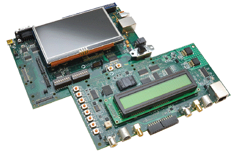
图2.ZOOM OMAP-L138 EVM开发套件外形图
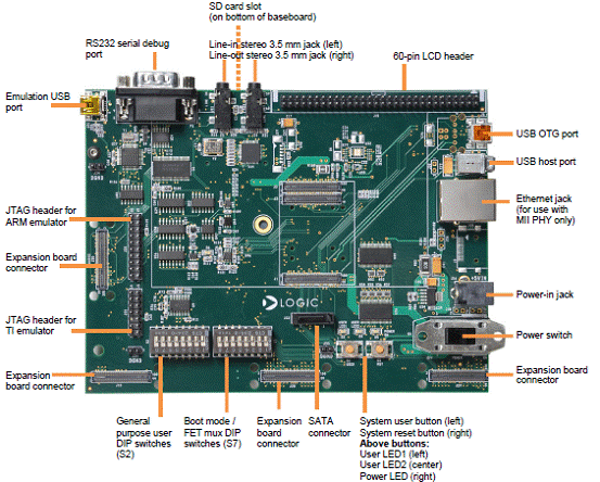
图3.ZOOM OMAP-L138 EVM开发套件应用基板外形图

图4.ZOOM OMAP-L138 EVM开发套件用户接口板外形图
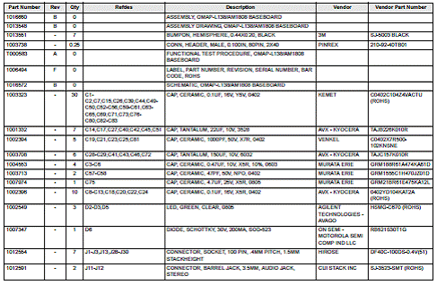
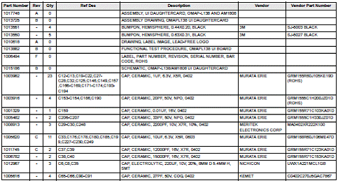
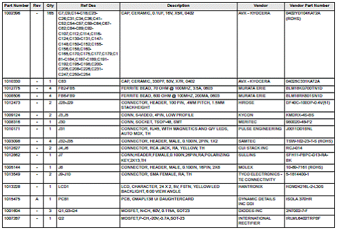
应用基板电材料清单:
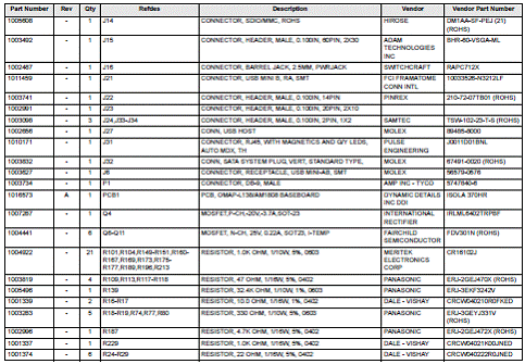


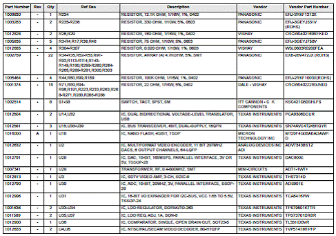
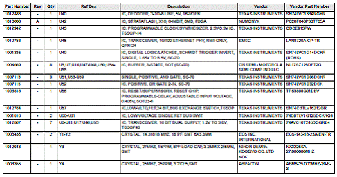
用户接口板材料清单:

责任编辑:HanFeng
【免责声明】
1、本文内容、数据、图表等来源于网络引用或其他公开资料,版权归属原作者、原发表出处。若版权所有方对本文的引用持有异议,请联系拍明芯城(marketing@iczoom.com),本方将及时处理。
2、本文的引用仅供读者交流学习使用,不涉及商业目的。
3、本文内容仅代表作者观点,拍明芯城不对内容的准确性、可靠性或完整性提供明示或暗示的保证。读者阅读本文后做出的决定或行为,是基于自主意愿和独立判断做出的,请读者明确相关结果。
4、如需转载本方拥有版权的文章,请联系拍明芯城(marketing@iczoom.com)注明“转载原因”。未经允许私自转载拍明芯城将保留追究其法律责任的权利。
拍明芯城拥有对此声明的最终解释权。
相关资讯
:
基于MC33771主控芯片的新能源锂电池管理系统解决方案

AMIC110 32位Sitara ARM MCU开发方案

基于AMIC110多协议可编程工业通信处理器的32位Sitara ARM MCU开发方案

基于展讯SC9820超低成本LTE芯片平台的儿童智能手表解决方案

基于TI公司的AM437x双照相机参考设计

基于MTK6580芯片的W2智能手表解决方案


 2012- 2022 拍明芯城ICZOOM.com 版权所有 客服热线:400-693-8369 (9:00-18:00)


