


 产品分类
产品分类
基于TI公司的DM388 IP照相机参考设计
 208
208
 拍明
拍明
原标题:TI DM388 IP照相机参考设计
TI公司的DM385和DM388是 DaVinci数字媒体处理器,采用ARMv7架构和高达1000MHz的ARM® Cortex™-A8 RISC处理器,高达2000 ARM Cortex-A8 MIPS和ARM Cortex-A8内核,具有高度集成成本效益和低功耗可编程的平台,满足HD视频会议-Skype终端, IP Netcam, 数字标牌,媒体播放器和适配器,移动医疗图像,网络投映仪,家庭音频和视频设备,以及具有SD,HD和4kx2k分辨率的同类设备所需的处理能力.本文介绍了DM385和DM388主要特性,框图, 以及DM388 IP照相机参考设计主要特性,电路图和材料清单.
DM385 and DM388 DaVinci Digital Media Processors are a highly integrated, cost-effective, low-power, programmable platform that leverages TI’s DaVinci processor technology to meet the processing needs of HD Video Conferencing - Skype endpoints, IP Netcam, Digital Signage, Media Players and Adapters, Mobile Medical Imaging, Network Projectors, Home Audio and Video Equipment, and similar devices in SD, HD, and 4K x 2K resolutions. The Programmable High-Definition Video Image Processor of the device supports 1080p60 of real time H.264BP/MP/HP video encode or decode. The included best-in-class H.264 encoder provides high-quality video encode for the lowest possible bit rate under all conditions, reducing valuable storage space to a minimum. In addition, the device also supports other video codecs such as MJPEG, MPEG-2, and MPEG-4. The device provides a full set of video preprocessing and postprocessing functions to ensure the best video quality. The low power consumption and high performance of the device makes it particularly suitable for portable and automotive applications. The DM388 is uniquely capable of running the Fourth-Generation Motion-Compensated Noise Filtering technology of TI.
The device enables original-equipment manufacturers (OEMs) and original-design manufacturers (ODMs) to quickly bring to market devices featuring robust operating systems support, rich user interfaces, and high processing performance through the maximum flexibility of a fully integrated mixed processor solution. The device also combines programmable video and audio processing with a highly integrated peripheral set.
The device processors include a high-definition video and imaging coprocessor 2 (HDVICP2), to off-load many video and imaging processing tasks for common video and imaging algorithms. Programmability is provided by an ARM Cortex-A8 RISC CPU with NEON extension and high-definition video and imaging coprocessors. The ARM lets developers separate control functions from A/V algorithms programmed on coprocessors, thus reducing the complexity of the system software. The ARM Cortex-A8 32-bit RISC processor with NEON floating-point extension includes: 32KB of instruction cache; 32KB of data cache; 256KB of L2 cache with ECC; 48KB of boot ROM; and 64KB of RAM.
The rich peripheral set provides the ability to control external peripheral devices and communicate with external processors. For details on each peripheral, see the related sections in this document and the associated peripheral reference guides. The peripheral set includes: HD Video Processing Subsystem; Dual-Port Gigabit Ethernet MACs (10/100/1000 Mbps) (Ethernet Switch) with MII/RMII/GMII/RGMII and MDIO interface supporting IEEE 1588 Time-Stamping, and Industrial Ethernet Protocols; two USB ports with integrated 2.0 PHY; PCIe x1 GEN2-Compliant interface; two serializer McASP audio serial ports (with DIT mode); three UARTs with IrDA and CIR support; four SPI serial interfaces; a CSI2 serial connection; three MMC/SD/SDIO serial interfaces; four I2C master and slave interfaces; a parallel camera interface (CAM); up to 125 general-purpose I/Os (GPIOs); eight 32-bit general-purpose timers; system watchdog timer; DDR2/DDR3/DDR3L SDRAM interface; flexible 8- or 16-bit asynchronous memory interface; a Spin Lock; and Mailbox.
Additionally, TI provides a complete set of development tools for the ARM which include C compilers and a Microsoft® Windows® debugger interface for visibility into source code execution.
DM385和DM388主要特性:
High-Performance DaVinci Digital Media Processors
Up to 1000-MHz ARM® Cortex™-A8 RISC Processor
Up to 2000 ARM Cortex-A8 MIPS
ARM Cortex-A8 Core
ARMv7 Architecture
In-Order, Dual-Issue, Superscalar Processor Core
NEON™ Multimedia Architecture
Supports Integer and Floating Point
Jazelle® RCT Execution Environment
ARM Cortex-A8 Memory Architecture
32KB of Instruction and Data Caches
256KB of L2 Cache with ECC
64KB of RAM, 48KB of Boot ROM
256KB of On-Chip Memory Controller (OCMC) RAM
Imaging Subsystem (ISS)
Camera Sensor Connection
Parallel Connection for Raw (up to 16-Bit) and BT.656/BT.1120 (8- or 16-Bit)
CSI2 Serial Connection
Image Sensor Interface (ISIF) for Handling Image and Video Data From the Camera Sensor
Image Pipe Interface (IPIPEIF) for Image and Video Data Connection Between Camera Sensor, ISIF, IPIPE, and DRAM
Image Pipe (IPIPE) for Real-Time Image and Video Processing
Resizer
Resizing Image and Video From 1/16x to 8x
Generating Two Different Resizing Outputs Concurrently
Hardware 3A Engine (H3A) for Generating Key Statistics for 3A (AE, AWB, and AF) Control
Face Detect (FD) Engine
Hardware Face Detection for up to 35 Faces Per Frame
Programmable High-Definition Video Image Coprocessing (HDVICP v2) Engine
Encode, Decode, Transcode Operations
H.264 BP/MP/HP, MPEG-2, VC-1, MPEG-4 SP/ASP, JPEG/MJPEG
Fourth-Generation Motion-Compensated Noise Filter (DM388 Only)
Media Controller
Controls the HDVPSS, HDVICP2, and ISS
Endianness
ARM Instructions and Data – Little Endian
HD Video Processing Subsystem (HDVPSS)
Two 165-MHz HD Video Capture Inputs
One 16- or 24-Bit Input, Splittable Into Dual 8-Bit SD Capture Ports
One 8-, 16-, or 24-Bit HD Input and 8-Bit SD Input Capture Port
Two 165-MHz HD Video Display Outputs
One 16-, 24-, or 30-Bit and One 16- or 24-Bit Output
Component HD Analog Output
Composite Analog Output
Digital HDMI 1.3 Transmitter with Integrated PHY
Advanced Video Processing Features Such as Scan, Format, and Rate Conversion
Three Graphics Layers and Compositors
32-Bit DDR2, DDR3, and DDR3L SDRAM Interface
Supports up to 400 MHz for DDR2, 533 MHz for DDR3, and 533 MHz for DDR3L
Up to Two x 16 Devices, 2GB of Total Address Space
Dynamic Memory Manager (DMM)
Programmable Multi-Zone Memory Mapping
Enables Efficient 2D Block Accesses
Supports Tiled Objects in 0°, 90°, 180°, or 270° Orientation and Mirroring
General-Purpose Memory Controller (GPMC)
8- or 16-Bit Multiplexed Address and Data Bus
512MB of Total Address Space Divided Among up to 8 Chip Selects
Glueless Interface to NOR Flash, NAND Flash (BCH/Hamming Error Code Detection), SRAM and Pseudo-SRAM
Error Locator Module (ELM) Outside of GPMC to Provide up to 16-Bit or 512-Byte Hardware ECC for NAND
Flexible Asynchronous Protocol Control for Interface to FPGA, CPLD, ASICs, and More
Enhanced Direct Memory Access (EDMA) Controller
Four Transfer Controllers
64 Independent DMA Channels
8 QDMA Channels
Ethernet Switch with Dual 10-, 100-, or
1000-Mbps External Interfaces (EMAC Software)
IEEE 802.3 Compliant (3.3-V I/O Only)
MII/RMII/GMII/RGMII Media Independent Interfaces
Management Data I/O (MDIO) Module
Reset Isolation
IEEE 1588 Time-Stamping and Industrial Ethernet Protocols
Dual USB 2.0 Ports with Integrated PHYs
USB2.0 High- and Full-Speed Clients
USB2.0 High-, Full-, and Low-Speed Hosts
Supports End Points 0-15
One PCI Express 2.0 Port with Integrated PHY
Supported on
All DM385 Devices
DM388 Devices with PCIe Enabled
Single Port with 1 Lane at 5.0 GT/s
Configurable as Root Complex or Endpoint
Eight 32-Bit General-Purpose Timers (Timer1–8)
One System Watchdog Timer (WDT0)
Three Configurable UART/IrDA/CIR Modules
UART0 with Modem Control Signals
Supports up to 3.6864 Mbps
SIR, MIR, FIR (4.0 MBAUD), and CIR
Four Serial Peripheral Interfaces (SPIs) (up to 48 MHz)
Each with Four Chip Selects
Three MMC/SD/SDIO Serial Interfaces (up to 48 MHz)
Supporting up to 1-, 4-, or 8-Bit Modes
Four Inter-Integrated Circuit (I2C Bus™) Ports
Two Multichannel Audio Serial Ports (McASP)
Six Serializer Transmit and Receive Ports
Two Serializer Transmit and Receive Ports
DIT-Capable For S/PDIF (All Ports)
Four Audio Tracking Logic (ATL) Modules
Real-Time Clock (RTC)
One-Time or Periodic Interrupt Generation
Up to 125 General-Purpose I/O (GPIO) Pins
One Spin Lock Module with up to 128 Hardware Semaphores
One Mailbox Module with 12 Mailboxes
On-Chip ARM ROM Bootloader (RBL)
Power, Reset, and Clock Management
SmartReflex™ Technology (Level 2b)
Multiple Independent Core Power Domains
Multiple Independent Core Voltage Domains
Support for Multiple Operating Points per Voltage Domain
Clock Enable and Disable Control for Subsystems and Peripherals
32KB of Embedded Trace Buffer™ (ETB™) and 5-pin Trace Interface for Debug
IEEE 1149.1 (JTAG) Compatible
609-Pin Pb-Free BGA Package (AAR Suffix), 0.8-mm Effective Pitch with Via Channel Technology to Reduce PCB Cost (0.5-mm Ball Spacing)
45-nm CMOS Technology
1.8- and 3.3-V Dual Voltage Buffers for General I/O
DM385和DM388主要应用领域:
IP Netcam
Video IP Phones
Embedded USB Encoding Cameras
All Camera Applications
HD Video Conferencing - Skype Endpoints
Digital Signage
Media Players and Adapters
Mobile Medical Imaging
Network Projectors
Home Audio and Video Equipment
Embedded Vision
Portable Medical Imaging and Diagnostics and Patient Monitoring
Remote Media Display
Thin Clients
Camcorders
Digital Scanner
Video Doorbells
Digital Photo Frames
Intrusion Control Panels with Video
Access Control Panels with Video
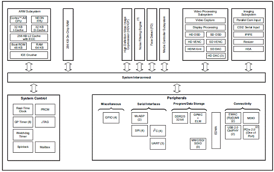
图1. DM385和DM388框图
Texas Instruments offers multiple highly optimized reference designs based on the DM36x, DM38x, DM812x, and DMVAx DaVinci™ video processors for the IP camera market to enable developers to speed through the design process as well as reducing overall bill of materials costs.
These reference designs:
Reduce development time by up 90%
Deliver higher quality video, up to 10 megapixel at reduced frame rate
Optimize electronic bill of materials
Empower customers to design sub $100 HD IP cameras
These solutions reduce development time by including:
Complete and optimized schematics
Gerber files
Free Linux application source code
Video Content Analysis (VCA) capability
DM388 IP照相机参考设计
Single platform solution provides SVCT/H.264 1080P 60 fps + SVCT/H.264 D1 30 fps + MJPEG 1080P 5 fps, and up to 10 megapixels at reduced frame rate. Supports TI’s 4th Generation Noise Filter and Local tone mapping dual frame merged WDR together with SVCT/H.264 1080P 30 fps.
DM388 IP照相机参考设计主要特性:
Processor: | DM388 DaVinci™ video processor includes ARM® Cortex™-A8, SVCT/H.264/MJPEG video coprocessor, Noise Filtering Engine and Gigabit EMAC |
Sensor: | Sony 2MP IMX136 sensor CMOS imager optimized for low-light performance (More Sensor Modules available from Leopard Imaging) |
Source Code: | Complete Linux-based IP camera application including free source code |
Video codecs: | Encode up to SVCT or H.264 high profile Level 3.1 1080p at >60fps including MPEG-4 and MJPEG support or higher megapixels at lower frame rate |
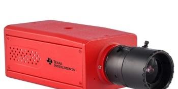
图2. TMDSIPCAM388X36 IP照相机外形图
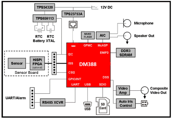
图3. TMDSIPCAM388X36 IP照相机参考设计电路图
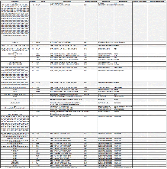
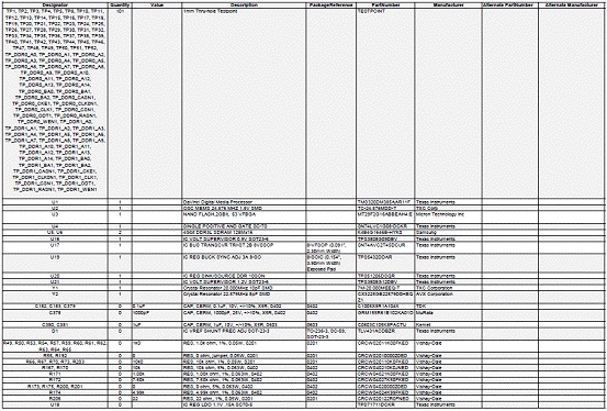
TMDSIPCAM388X36 IP照相机参考设计材料清单:
责任编辑:HanFeng
【免责声明】
1、本文内容、数据、图表等来源于网络引用或其他公开资料,版权归属原作者、原发表出处。若版权所有方对本文的引用持有异议,请联系拍明芯城(marketing@iczoom.com),本方将及时处理。
2、本文的引用仅供读者交流学习使用,不涉及商业目的。
3、本文内容仅代表作者观点,拍明芯城不对内容的准确性、可靠性或完整性提供明示或暗示的保证。读者阅读本文后做出的决定或行为,是基于自主意愿和独立判断做出的,请读者明确相关结果。
4、如需转载本方拥有版权的文章,请联系拍明芯城(marketing@iczoom.com)注明“转载原因”。未经允许私自转载拍明芯城将保留追究其法律责任的权利。
拍明芯城拥有对此声明的最终解释权。
相关资讯
:
基于MC33771主控芯片的新能源锂电池管理系统解决方案

AMIC110 32位Sitara ARM MCU开发方案

基于AMIC110多协议可编程工业通信处理器的32位Sitara ARM MCU开发方案

基于展讯SC9820超低成本LTE芯片平台的儿童智能手表解决方案

基于TI公司的AM437x双照相机参考设计

基于MTK6580芯片的W2智能手表解决方案


 2012- 2022 拍明芯城ICZOOM.com 版权所有 客服热线:400-693-8369 (9:00-18:00)


