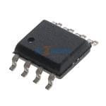
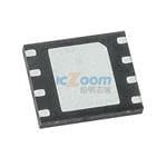
描述:
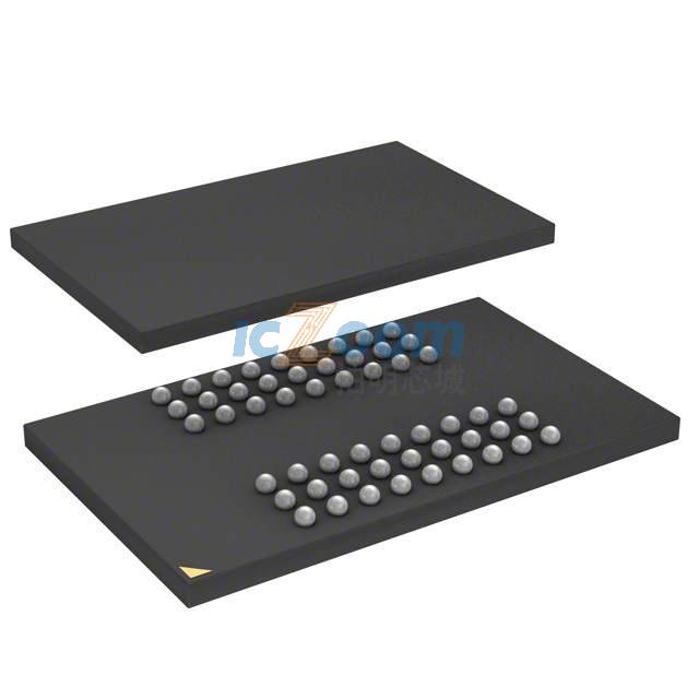
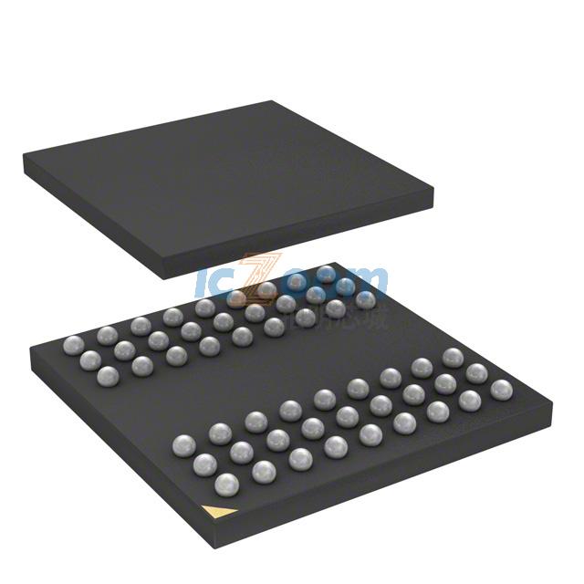
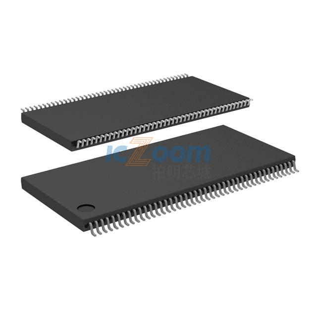
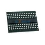
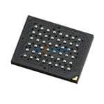
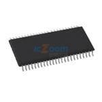
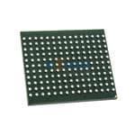
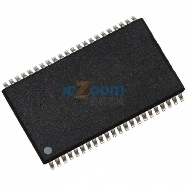
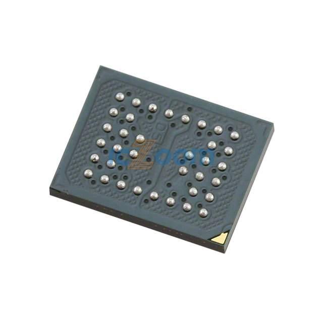
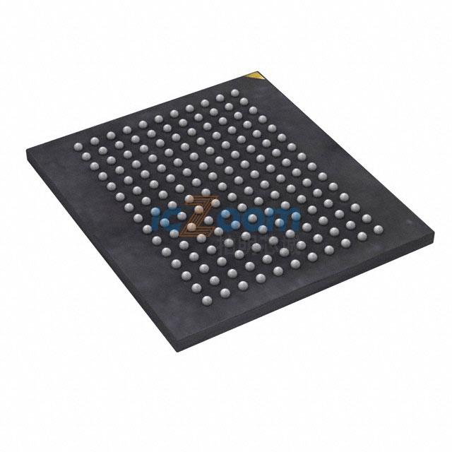
* Vdd = 1.8V ±0.1V, Vddq = 1.8V ±0.1V * JEDEC standard 1.8V I/O (SSTL_18-compatible) * Double data rate interface: two data transfers per Clock cycle * Differential data strobe (DQS, DQS) * 4-bit prefetch architecture * On chip DLL to align DQ and DQS transitions with CK * 8 internal banks for concurrent operation * Programmable CAS latency (CL) 3, 4, 5, 6, and 7 supported * Posted CAS and programmable additive latency (AL) 0, 1, 2, 3, 4, 5, and 6 supported * WRITE latency = READ latency - 1 tCK * Programmable burst lengths: 4 or 8 * Adjustable data-output drive strength, full and reduced strength options * On-die termination (ODT) * Configuration(s): 256Mx8 (32Mx8x8 banks) * Package: x8: 60-ball BGA (10.5mm x 13mm) x16: 84-ball WBGA (10.5mm x 13.5mm) * Temperature Range: Commercial (0°C ≤ Tc ≤ 85°C) Industrial (-40°C ≤ Tc ≤ 95°C; -40°C ≤ Ta ≤ 85°C) Tc = Case Temp, Ta = Ambient Temp


 产品分类
产品分类
 DRAM
DRAM


 2012- 2022 拍明芯城ICZOOM.com 版权所有 客服热线:400-693-8369 (9:00-18:00)


