


 产品分类
产品分类
Intel Stratix 10 SoC FPGA系列开发方案
 424
424
 拍明
拍明
原标题:Intel Stratix 10 SoC FPGA系列开发方案
Intel公司的Stratix 10 SoC FPGA系列采用14nm三栅极(FinFET)和异构三维封装系统工艺技术,比以前高性能SoC FPGA提供2x核性能和节省多达70%的功耗, 单片核架构多达550万个逻辑单源(LE),多达96个全双工收发器通路,收发器数据速率高达28.3Gbps,嵌入eSRAM (45 Mbit)和M20K (20 kbit)SRAM存储器区块,基于PLL的分数合成和超低抖动LC振荡器,硬PCI Express® Gen3 x16 IP区块,每个收发器通路中有硬10GBASE-KR/40GBASE-KR4 FEC,每个引脚的硬存储器控制器和PHY支持DDR4速率高达2666Mbps,以及硬定点和IEEE 754兼容硬浮点可变精度数字信号处理(DSP)区块,计算功能达10 TFLOPS,主要用在计算和存储,网络,光传输网络,广播和军用雷达和保密通信,医疗诊断扫描和图像,测试测量以及无线5G网络等.本文介绍了Stratix 10 SoC FPGA器件主要特性和创新要点,框图,以及Stratix 10 SoC FPGA开发板主要特性,框图和电路图.
Intel ’s 14-nm Intel Stratix 10 SX SoCs deliver 2x core performance and up to 70% lower power over previous generation high-performance SoCs. Featuring several groundbreaking innovations, including the all new Intel Hyperflex™ core architecture,this device family enables you to meet the demand for ever-increasing bandwidth and processing performance in you most advanced applications, while meeting your power budget.
Featuring several groundbreaking innovations, including the all new HyperFlex™ core architecture, this device family enables you to meet the demand for ever-increasing bandwidth and processing performance in your most advanced applications, while meeting your power budget.
With an embedded hard processor system (HPS) based on a quad-core 64-bit ARM® Cortex®-A53, the Stratix 10 SoC devices deliver power efficient, application-class processing and allow designers to extend hardware virtualization into the FPGA fabric.Stratix 10 SoC devices demonstrate Intel’s commitment to high-performance SoCs and extend Intel’s leadership in programmable devices featuring an ARM-based processor system.
Important innovations in Stratix 10 FPGAs and SoCs include:
• All new HyperFlex core architecture delivering 2X the core performance compared to previous generation high-performance FPGAs
• Industry leading Intel 14-nm Tri-Gate (FinFET) technology
• Heterogeneous 3D System-in-Package (SiP) technology
• Monolithic core fabric with up to 5.5 million logic elements (LEs)
• Up to 96 full duplex transceiver channels on heterogeneous 3D SiP transceiver tiles
• Transceiver data rates up to 28.3 Gbps chip-to-chip/module and backplane
performance
• Embedded eSRAM (45 Mbit) and M20K (20 kbit) internal SRAM memory blocks
• Fractional synthesis and ultra-low jitter LC tank based transmit phase locked loops
(PLLs)
• Hard PCI Express® Gen3 x16 intellectual property (IP) blocks
• Hard 10GBASE-KR/40GBASE-KR4 Forward Error Correction (FEC) in every
transceiver channel
• Hard memory controllers and PHY supporting DDR4 rates up to 2666 Mbps per pin
• Hard fixed-point and IEEE 754 compliant hard floating-point variable precision digital signal processing (DSP) blocks with up to 10 TFLOPS compute performance with a power efficiency of 80 GFLOPS per Watt
• Quad-core 64-bit ARM Cortex-A53 embedded processor running up to 1.5 GHz in
SoC family variants
• Programmable clock tree synthesis for flexible, low power, low skew clock trees
• Dedicated secure device manager (SDM) for:
— Enhanced device configuration and security
— AES-256, SHA-256/384 and ECDSA-256/384 encrypt/decrypt accelerators and
authentication
— Multi-factor authentication
— Physically Unclonable Function (PUF) service and software programmable device configuration capability
• Comprehensive set of advanced power saving features delivering up to 70% lower
power compared to previous generation high-performance FPGAs
• Non-destructive register state readback and writeback, to support ASIC prototyping and other applications
Stratix 10 SoC FPGA应用:
With these capabilities, Stratix 10 FPGAs and SoCs are ideally suited for the most
demanding applications in diverse markets such as:
• Compute and Storage—for custom servers, cloud computing and data center acceleration
• Networking—for Terabit, 400G and multi-100G bridging, aggregation, packet processing and traffic management
• Optical Transport Networks—for OTU4, 2xOTU4, 4xOTU4
• Broadcast—for high-end studio distribution, headend encoding/decoding, edge
quadrature amplitude modulation (QAM)
• Military—for radar, electronic warfare, and secure communications
• Medical—for diagnostic scanners and diagnostic imaging
• Test and Measurement—for protocol and application testers
• Wireless—for next-generation 5G networks
• ASIC Prototyping—for designs that require the largest monolithic FPGA fabric with the highest I/O count
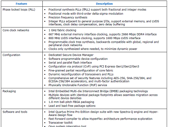
Stratix 10 SoC FPGA器件主要特性:


Stratix 10 SoC FPGA器件子系统主要特性:
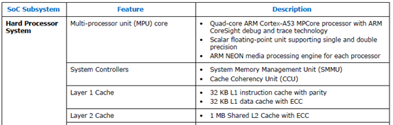
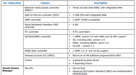

图1. Stratix 10 SoC FPGA器件框图
Stratix 10 SoC FPGA开发板
The Intel® Stratix® 10 SoC Development Kit offers a quick and simple approach for developing custom ARM* processor-based SoC designs. The Stratix 10 SoCs offer full software compatibility with previous generation SoCs, a broad ecosystem of ARM software and tools, and the enhanced FPGA and digital signal processing (DSP) hardware design flow.
The Intel Stratix 10 SoC development board provides a hardware platform for developing and prototyping low-power, high-performance and logic-intensive designs using Intel Stratix 10 SoC. The board provides a wide range of peripherals and memory interfaces to facilitate the development of Intel Stratix 10 SoC designs.
图2. Stratix 10 SoC FPGA开发板框图
Stratix 10 SoC FPGA开发板包括:

Stratix 10 SoC FPGA开发板主要特性:
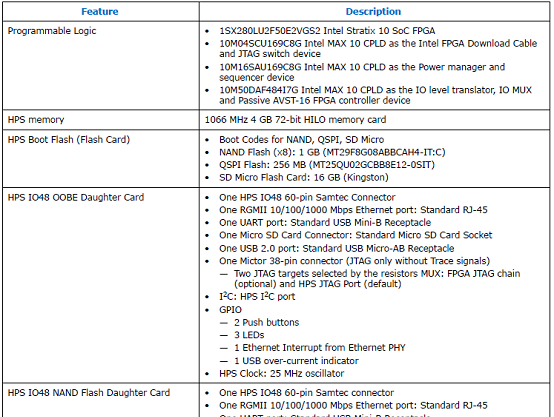
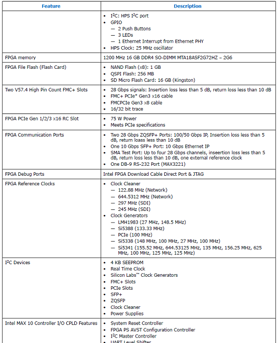
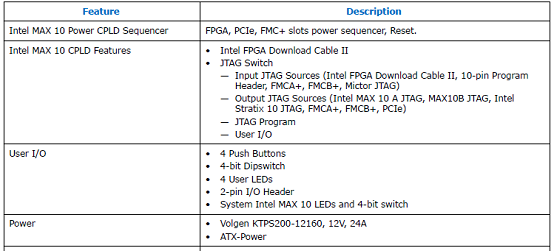

图3. Stratix 10 SoC FPGA开发板外形图(正面)

图4. Stratix 10 SoC FPGA开发板外形图(背面)
责任编辑:HanFeng
【免责声明】
1、本文内容、数据、图表等来源于网络引用或其他公开资料,版权归属原作者、原发表出处。若版权所有方对本文的引用持有异议,请联系拍明芯城(marketing@iczoom.com),本方将及时处理。
2、本文的引用仅供读者交流学习使用,不涉及商业目的。
3、本文内容仅代表作者观点,拍明芯城不对内容的准确性、可靠性或完整性提供明示或暗示的保证。读者阅读本文后做出的决定或行为,是基于自主意愿和独立判断做出的,请读者明确相关结果。
4、如需转载本方拥有版权的文章,请联系拍明芯城(marketing@iczoom.com)注明“转载原因”。未经允许私自转载拍明芯城将保留追究其法律责任的权利。
拍明芯城拥有对此声明的最终解释权。
相关资讯
:
基于MC33771主控芯片的新能源锂电池管理系统解决方案

AMIC110 32位Sitara ARM MCU开发方案

基于AMIC110多协议可编程工业通信处理器的32位Sitara ARM MCU开发方案

基于展讯SC9820超低成本LTE芯片平台的儿童智能手表解决方案

基于TI公司的AM437x双照相机参考设计

基于MTK6580芯片的W2智能手表解决方案


 2012- 2022 拍明芯城ICZOOM.com 版权所有 客服热线:400-693-8369 (9:00-18:00)


