TI BQ25618/BQ25619 I2C控制的1.5A单电池充电器解决方案
 311
311
 拍明
拍明
原标题:TI BQ25618/619 I2C控制的1.5A单电池充电器解决方案
TI公司的BQ25618/BQ25619是I2C控制的1.5A单电池充电器,单个器件集成了充电升压转换器和电压保护,提供了业界最低的端电流,用来给可穿戴设备进行全电池容量充电.在芯片模式,BQ25618/619业界最好的低静态电流把电池漏电流降低到6uA,使得电池能量双倍于设备的保存期.器件是用于锂电池和锂聚合电池的高度集成的1.5A开关模式电池充电管理和系统电源通路管理设备.具有快速充电和高输入电压,支持各种应用包括可穿戴设备和耳机充电.它的低阻抗功率通路优化了开关模式操作效率,降低电池充电时间和在放电时扩展了电池运行时间.电池遥测提供了电池最大充电功率.器件高度集成了输入反向阻隔FET(RBFET,Q1),高边开关FET(HSFET,Q2),低边开关FET(LSFET,Q3)以及电池FET(BATFET,Q4).它还集成了用于高边栅驱动的自举电路,从而简化了系统设计.I2C串行接口带有充电和系统设定,使得设备是真正的灵活的解决方案.器件工作频率1.5MHz,0.5A时充电效率95.5%,1A时为94.5%,充电电压调节±0.5%(每步10mV).主要用在消费类电子如可穿戴设备等.本文介绍了BQ25618/619主要特性,框图,典型应用电路,以及评估模块BMS024 EVM测试建立图,电路图,材料清单和PCB设计图.
The BQ25618/619 integrates charge, boost converter and voltage protection in a single device. It offers theindustry’s lowest termination current for switchingchargers to charge wearable devices by full batterycapacity. The BQ25618/619 best-in-class lowquiescent current reduces battery leakage down to 6uA in ship mode, which conserves battery energy todouble the shelf life for the device. BQ25619 is in 4x4QFN package for easy layout. BQ25618 is in2.0x2.4mm2 WCSP package for space limited design.
The BQ25619/618 is a highly integrated 1.5-A switch-mode battery charge management and system Power Pathmanagement device for Li-Ion and Li-polymer battery. It features fast charging with high input voltage support fora wide range of applications including wearables, and earphone charging case. Its low impedance power pathoptimizes switch-mode operation efficiency, reduces battery charging time and extends battery run time duringdischarging phase. Its input voltage and current regulation, low termination current, and battery remote sensingdeliver maximum charging power to the battery. The solution is highly integrated with input reverse-blocking FET(RBFET, Q1), high-side switching FET (HSFET, Q2), low-side switching FET (LSFET, Q3), and battery FET(BATFET, Q4) between system and battery. It also integrates the bootstrap diode for the high-side gate drive forsimplified system design. The I2C serial interface with charging and system settings makes the device a trulyflexible solution.
The device supports a wide range of input sources, including standard USB host port, USB charging port, USBcompliant high voltage adapter and wireless power. It is compliant with USB 2.0 and USB 3.0 power spec withinput current and voltage regulation. The device takes the result from detection circuit in the system, such asUSB PHY device.
The device integrates the buck charger and boost regulator into one solution with single inductor. The boostmode supplies 5V (adjustable 4.6 V/4.75 V/5 V/5.15 V) on PMID pin. The boost mode is used to save BOM andcharge another battery by the control of PMID_GOOD.The PMID_GOOD pin is used to drive the external PMOSFET to disconnect boost output PMID from the attached accessories.
The device initiates and completes a charging cycle without software control. It senses the battery voltage andcharges the battery in three phases: pre-conditioning, constant current and constant voltage. At the end of thecharging cycle, the charger automatically terminates when the charge current is below a preset limit and thebattery voltage is higher than the recharge threshold. If the fully charged battery falls below the rechargethreshold, the charger automatically starts another charging cycle.
The BQ2619 device is available in 24-pin, 4 mm × 4 mm x 0.75 mm thin WQFN package and BQ25618 isavailable in 30-ball, 2.0 mm × 2.4 mm WCSP package. The BQ25619/618 is a highly integrated 1.5-A switch-mode battery charge management and system Power Pathmanagement device for Li-Ion and Li-polymer battery. It features fast charging with high input voltage support fora wide range of applications including wearables, and earphone charging case. Its low impedance power pathoptimizes switch-mode operation efficiency, reduces battery charging time and extends battery run time duringdischarging phase. Its input voltage and current regulation, low termination current, and battery remote sensingdeliver maximum charging power to the battery. The solution is highly integrated with input reverse-blocking FET(RBFET, Q1), high-side switching FET (HSFET, Q2), low-side switching FET (LSFET, Q3), and battery FET(BATFET, Q4) between system and battery. It also integrates the bootstrap diode for the high-side gate drive forsimplified system design. The I2C serial interface with charging and system settings makes the device a trulyflexible solution.
The Power Path management regulates the system slightly above battery voltage but does not drop below 3.5-Vminimum system voltage (programmable) with adapter applied. With this feature, the system maintains operationeven when the battery is completely depleted or removed. When the input current limit or voltage limit is reached,the Power Path management automatically reduces the charge current. As the system load continues toincrease, the battery starts to discharge the battery until the system power requirement is met. This supplementmode prevents overloading the input source.
The device initiates and completes a charging cycle without software control. It senses the battery voltage andcharges the battery in three phases: pre-conditioning, constant current and constant voltage. At the end of thecharging cycle, the charger automatically terminates when the charge current is below a preset limit and thebattery voltage is higher than the recharge threshold. If the fully charged battery falls below the recharge threshold, the charger automatically starts another charging cycle.
The charger provides various safety features for battery charging and system operations, including batterynegative temperature coefficient thermistor monitoring, charging safety timer and overvoltage and over-currentprotections. Thermal regulation reduces charge current when the junction temperature exceeds 110°C. Thestatus register reports the charging status and any fault conditions. With I2C, the VBUS_GD bit indicates if agood power source is present, and the INT output immediately notifies host when a fault occurs.
The device also provides the QON pin for BATFET enable and reset control to exit low power ship mode or fullsystem reset function.
The BQ2619 device is available in 24-pin, 4 mm × 4 mm x 0.75 mm thin WQFN package and BQ25618 isavailable in 30-ball, 2.0 mm × 2.4 mm WCSP package.
BQ25618/619主要特性:
• Single chip solution to charge wearableaccessories from adapter or battery
• High-efficiency, 1.5-MHz, synchronous switchmodebuck charger
– 95.5% Charge efficiency at 0.5 A and 94.5%efficiency at 1 A
– ±0.5% Charge voltage regulation (10-mV step)
– I2C Programmable JEITA profile of chargevoltage, current and temperature thresholds
– Low termination current with high accuracy 20mA±10 mA
– Small inductor form factor of 2.5x2.0x1.0 mm3
• Boost mode with output from 4.6 V to 5.15 V
– 94% Boost efficiency at 1-A output
– Integrated control to switch between chargeand boost mode
– PMID_GOOD Pin control external PMOS FETfor protection against fault conditions
• Single input to support USB input and highvoltageadapter and wireless power
– Support 4-V to 13.5-V input voltage range with22-V absolute max input rating
– Programmable input current limit (IINDPM)with I2C (100-mA to 3.2-A, 100-mA/step)
– Maximum power tracking by input voltage limit(VINDPM) up to 5.4 V
– VINDPM Threshold automatically tracksbattery voltage
• Narrow VDC (NVDC) power path management
– System instant-on with no battery or deeplydischarged battery
• Flexible I2C configuration and autonomouscharging for optimal system performance
• High integration includes all MOSFETs, currentsensing and loop compensation
• Low Rdson 19.5-mΩ BATFET to minimizecharging loss and extend battery run time
– BATFET Control for ship mode, and fullsystem reset with and without adapter
• 7-μA Low battery leakage current in ship mode
• 9.5-μA Low battery leakage current with systemstandby
• High accuracy battery charging profile
– ±6% Charge current regulation
– ±7.5% Input current regulation
– Remote battery sensing to charge faster
– Programmable top-off timer for full batterycharging
BQ25618/619应用:
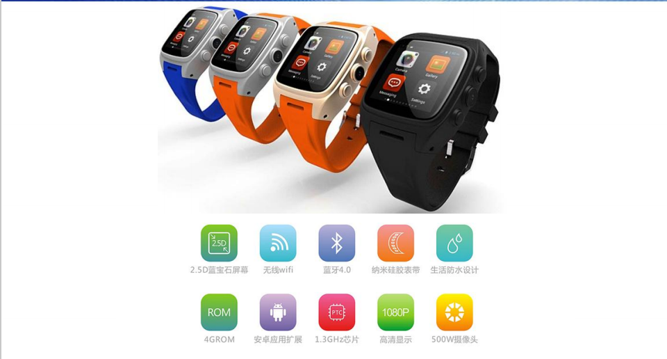
• Consumer wearables, smartwatch
• Personal care and fitness
• Headsets/headphone
• Earbuds (True Wireless or TWS) charging case
• Hearing aids charging case
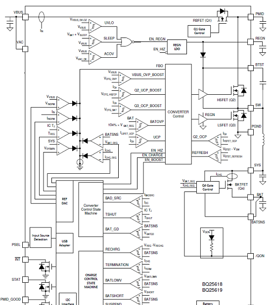
图1.BQ25618/619功能框图

图2.BQ25618/619简化应用电路图
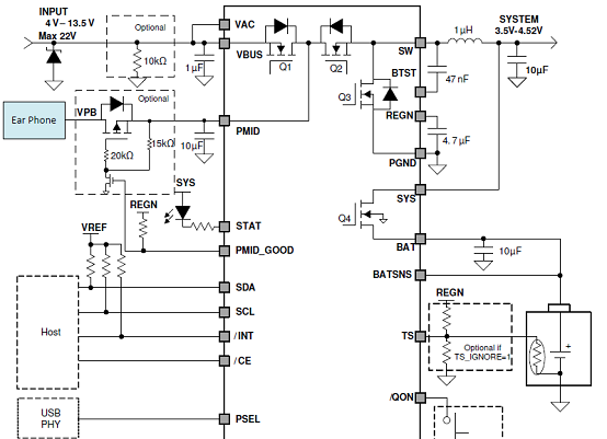
图3.BQ25619和PMOS应用电路图
BQ25618评估模块BMS024 EVM
The BMS024 evaluation module (EVM) is a complete charger module for evaluating an I2C-controlledsingle-cell NVDC charger using any of the devices listed above.
This EVM does not include the EV2300/EV2400 interface board. To evaluate the EVM, an EV2300/EV2400 interface board must be ordered separately.
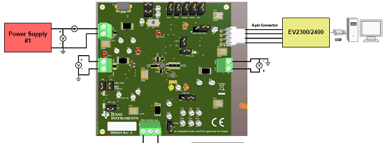
图4.评估模块BMS024 EVM测试建立图
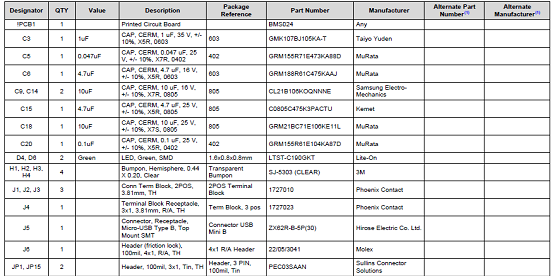
评估模块BMS024 EVM材料清单:


责任编辑:David
【免责声明】
1、本文内容、数据、图表等来源于网络引用或其他公开资料,版权归属原作者、原发表出处。若版权所有方对本文的引用持有异议,请联系拍明芯城(marketing@iczoom.com),本方将及时处理。
2、本文的引用仅供读者交流学习使用,不涉及商业目的。
3、本文内容仅代表作者观点,拍明芯城不对内容的准确性、可靠性或完整性提供明示或暗示的保证。读者阅读本文后做出的决定或行为,是基于自主意愿和独立判断做出的,请读者明确相关结果。
4、如需转载本方拥有版权的文章,请联系拍明芯城(marketing@iczoom.com)注明“转载原因”。未经允许私自转载拍明芯城将保留追究其法律责任的权利。
拍明芯城拥有对此声明的最终解释权。


 产品分类
产品分类








 2012- 2022 拍明芯城ICZOOM.com 版权所有 客服热线:400-693-8369 (9:00-18:00)


