Freescale MM912F634汽车继电器驱动和LIN连接解决方案
 213
213
 拍明
拍明
原标题:Freescale MM912F634汽车继电器驱动和LIN连接解决方案
freescale公司的MM912F634是S12 MagniV系列产品中一员,集成了继电器驱动以及LIN收发器. 器件采用16位S12 CPU,具有32KB闪存和2.0KB RAM,背景调试(BDM)和调试模块(DBG),带SCI的LIN 2.1物理层接口,10位15通路的ADC,16位4通路的定时器模块(TIM16B4C),8位2路PWM,六种高压/叫醒输入和三个低压GPIO,主要用在汽车的门窗提升和座位控制以及LIN连接.本文介绍了MM912F634主要特性,方框图,简化应用电路以及评估板KIT912F634EVME主要特性,电路图和材料清单(BOM).
The MM912_634 is part of the S12 MagniV portfolio which simplifies system design with easy-to-use, expertly integrated mixed-signal microcontrollers for automotive applications. This dual-die solution is built on proven S12 technology, enabling software and tool compatibility across the entire portfolio. The SMARTMOS-based analog die combines System Basis Chip (SBC) functionality and application specific functions, which include a Local Interconnect Network (LIN) transceiver, relay drivers, a DC motor current sense circuit, and a selection of high and low side digital I/O. Control of the analog die is via a new high performance internal Die to Die interface (D2D), which seamlessly integrates the analog IC registers into the MCU register map, to provide faster access than SPI based systems.
The MM912F634 is an integrated single package solution that integrates an HCS12 microcontroller with a SMARTMOS analog control IC. The Die to Die Interface (D2D) controlled analog die combines system base chip and application specific functions, including a LIN transceiver.
MM912F634主要特性:
• 16-Bit S12 CPU, 32 kByte FLASH, 2.0 kByte RAM
• Background Debug (BDM) & Debug Module (DBG)
• Die to Die bus interface for transparent memory mapping
• On-chip oscillator & two independent watchdogs
• LIN 2.1 Physical Layer Interface with integrated SCI
• Six digital MCU GPIOs shared with SPI (PA5…0)
• 10-Bit, 15 Channel - Analog to Digital Converter (ADC)
• 16-Bit, 4 Channel - Timer Module (TIM16B4C)
• 8-Bit, 2 Channel - Pulse width modulation module (PWM)
• Six high voltage / Wake-up inputs (L5.0)
• Three low voltage GPIOs (PB2.0)
• Low Power Modes with cyclic sense & forced wake-up
• Current Sense Module with selectable gain
• Reverse Battery protected Voltage Sense Module
• Two protected low side outputs to drive inductive loads
• Two protected high side outputs
• Chip temperature sensor
• Hall sensor supply
• Integrated voltage regulator(s)
MM912F634目标应用:
Automotive:Doors, Window Lift and Seat Control
Connectivity :Local Interconnect Network (LIN)

图1.MM912F634方框图

图2.MM912F634电源电路图

图3.MM912F634简化应用电路图
评估板KIT912F634EVME
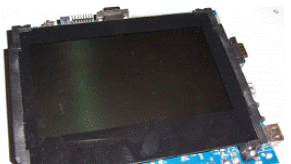
Freescale Semiconductor’s KIT912F634EVME is a system solution which gives the user the capability to easily evaluate most of the features provided by the MM912F634 - Integrated Dual Low Side and Dual High Side Switch with Embedded MCU and LIN Transceiver for Relay Drivers. The 912F634 features 2 die in a single package. The 16-bit core and the analog die are connected by means of the Die to Die interface that provides direct address access to the registers on the analog die. The analog die contains HS and LS switches, as well as a PWM module, ADC module, timer module, SCI module, LIN physical interface, and other general registers. All external signals are accessible via header connectors, and most of the signals can also be checked via test points. The evaluation module board also includes the TBDML programming/debugging interface, so no external interface is needed. The board can be powered either from two 4.0 mm banana connectors or from the LIN connector. For quick familiarization with the device, a graphical user interface, based on FreeMASTER software, is provided together with the module. Thanks to the GUI, the user can easy evaluate the peripheral modules, or directly access the registers on the analog die.
评估板KIT912F634EVME主要特性:
•16-Bit S12 CPU, 32 kByte FLASH, 2.0 kByte RAM
•Background Debug (BDM) & Debug Module (DBG)
•Die to Die bus interface for transparent memory mapping
•On-chip oscillator & two independent watchdogs
•LIN 2.1 Physical Layer Interface with integrated SCI
•Six digital MCU GPIOs shared with SPI (PA5…0)
•10-Bit, 15 Channel - Analog to Digital Converter (ADC)
•16-Bit, 4 Channel - Timer Module (TIM16B4C)
•8-Bit, 2 Channel - Pulse width modulation module (PWM)
•Six high voltage / Wake-up inputs (L5.0)
•Three low voltage GPIOs (PB2.0)
•Low Power Modes with cyclic sense & forced wake-up
•Current Sense Module with selectable gain
•Reverse Battery protected Voltage Sense Module
•Two protected low side outputs to drive inductive loads
•Two protected high side outputs
•Chip temperature sensor
•Hall sensor supply
•Integrated voltage regulator(s)

图4.评估板KIT912F634EVME外形图
评估板KIT912F634EVME材料清单(BOM):


责任编辑:HanFeng
【免责声明】
1、本文内容、数据、图表等来源于网络引用或其他公开资料,版权归属原作者、原发表出处。若版权所有方对本文的引用持有异议,请联系拍明芯城(marketing@iczoom.com),本方将及时处理。
2、本文的引用仅供读者交流学习使用,不涉及商业目的。
3、本文内容仅代表作者观点,拍明芯城不对内容的准确性、可靠性或完整性提供明示或暗示的保证。读者阅读本文后做出的决定或行为,是基于自主意愿和独立判断做出的,请读者明确相关结果。
4、如需转载本方拥有版权的文章,请联系拍明芯城(marketing@iczoom.com)注明“转载原因”。未经允许私自转载拍明芯城将保留追究其法律责任的权利。
拍明芯城拥有对此声明的最终解释权。


 产品分类
产品分类




 2012- 2022 拍明芯城ICZOOM.com 版权所有 客服热线:400-693-8369 (9:00-18:00)


