


 产品分类
产品分类
基于PLC541XX的OSRAM 穿戴式设备心率血氧检测解决方案
 240
240
 拍明
拍明
原标题:品佳集团力推 OSRAM 穿戴式设备心率血氧检测解决方案
【方案介绍】】
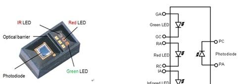
OSRAM在穿戴设备领域推出首款基于运动和健康监控应用的整合型光传感器SFH7050。尺寸仅4.7 毫米x2.5毫米x 0.9毫米,只需极小的功率和空间,因此非常适合用于智能手环、智能手表。使用者只要将搭载该款传感器的装置配戴于手腕或将手指放在感测器上,即可测得心率和血氧浓度。
SFH7050集成了绿光、红光、红外三颗LED 和一颗光电接收管。采用OSRAM专利Thin Firm技术的LED,光效高,可以在低功耗下运行;光电接收管具有高的光感灵敏度,可以进行精确的信号采集,为心率和血氧值的计算提供可靠信号源;另外红外LED与光电接收管可实现近接感测功能。
SFH7050作为检测心率和血氧的核心器件,我们推荐选用Microchip USB充电IC和LDO, 以及Bosch G-Sensor, NXP LPC54100系列微处理器作为整套穿戴设备设计的关键器件。
为了满足客户不同应用功能细分,在SFH7050的基础上,OSRAM已陆续推出结构优化和光效更高,专门针对心率测试功能的SFH7051和同时具备心率血氧测试功能的SFH7060。详细的功能和介绍可以联系品佳集团。
【方案特色】
SFH7050
• Multi chip package featuring 3 emitters and one detector;
• Small package:4.7mm*2.5mm*0.9mm;
• Light Barrier to block optical crosstalk.
【规格说明】

Target Application:
• Smart Watch;
• Smart Phone;
• Wearable Device, etc.
NXP PLC541XX
Overview
The LPC541xx MCU family of single-core and dual-core MCUs represents the next-generation of industry-leading power efficiency. With added scalability and feature integration, these breakthrough devices enable continued market growth in today's competitive always-on environment.
LPC541xx MCUs are based on the power-efficient Arm® Cortex-M4 core, each with an optional Cortex®-M0+ coprocessor. Single Cortex-M4 options are available for architectures that value single core processing without software partitioning.
In an always-on application, these MCUs operate in a power-down mode, listening for incoming data, which when available, can wake either core to acquire or process the information. When in an active mode, developers can optimize power efficiency and throughput by choosing between the power-efficient Cortex-M0+ core for data collection, aggregation, and system task management, or the Cortex-M4 core, which can complete processor-intensive algorithms, such as sensor fusion more quickly helping to reduce power consumed.
The optional dedicated on-chip digital microphone (DMIC) subsystem on the LPC54110 family will also dramatically reduce power in applications that demand voice input and processing, achieving the stringent power efficiencies required for always-on voice-activation in battery-operated products.
This device is fully supported by NXP’s MCUXpresso Software and Tools, a comprehensive and cohesive set of free software development tools for Kinetis, LPC and i.MX RT microcontrollers. MCUXpresso SDK also includes project files for Keil MDK and IAR EWARM.
Arm Cortex-M4 core (version r0p1)
Arm Cortex-M4 processor, running at a frequency of up to 100 MHz.
Floating Point Unit (FPU) and Memory Protection Unit (MPU).
Arm Cortex-M4 built-in Nested Vectored Interrupt Controller (NVIC).
Non-maskable Interrupt (NMI) input with a selection of sources.
Serial Wire Debug (SWD) with six instruction break points, two literal comparators, and four watchpoints. Includes Serial Wire Output for enhanced debug capabilities.
System tick timer.
Arm Cortex-M0+ core
Arm Cortex-M0+ processor, running at a frequency of up to 100 MHz (uses the same clock as Cortex-M4) with a single-cycle multiplier and a fast single-cycle I/O port.
Arm Cortex-M0+ built-in Nested Vectored Interrupt Controller (NVIC).
Non-maskable Interrupt (NMI) input with a selection of sources.
Serial Wire Debug with four breakpoints and two watchpoints.
System tick timer.
On-chip memory
Up to 256 KB on-chip flash program memory with the flash accelerator and 256-byte page erase and write.
Up to 192 KB total SRAM consisting of 160 KB contiguous main SRAM and an additional 32 KB SRAM on the I&D buses.
ROM API supports
Flash In-Application Programming (IAP) and In-System Programming (ISP).
ROM-based USB drivers (HID, CDC, MSC, and DFU). Flash updates via USB is supported.
Supports booting from valid user code in flash, USART, SPI, and I2C.
Legacy, Single, and Dual image boot.
Serial interfaces
Flexcomm Interface contains eight serial peripherals. Each can be selected by software to be a USART, SPI, or I2C interface. Two Flexcomm Interfaces also include an I2S interface. Each Flexcomm Interface includes a FIFO that supports USART, SPI, and I2S if supported by that Flexcomm Interface. A variety of clocking options are available to each Flexcomm Interface and include a shared fractional baud-rate generator.
I2C-bus interfaces support Fast-mode and Fast-mode Plus with data rates of up to 1Mbit/s and with multiple address recognition and monitor mode. Two sets of true I2C pads also support high-speed mode (3.4 Mbit/s) as a slave.
Crystal-less USB full-speed device interface.
Digital peripherals
DMA controller with 20 channels and 20 programmable triggers, able to access all memories and DMA-capable peripherals.
Up to 48 General-Purpose Input/Output (GPIO) pins. Most GPIOs have configurable pull-up/pull-down resistors, programmable open-drain mode, and input inverter.
GPIO registers are located on the AHB for fast access.
Up to eight GPIOs can be selected as pin interrupts (PINT), triggered by rising, falling or both input edges.
Two GPIO grouped interrupts (GINT) enable an interrupt based on a logical (AND/OR) combination of input states.
CRC engine.
Analog peripherals
12-bit ADC with 12 input channels and with multiple internal and external trigger inputs and sample rates of up to 5.0 MSamples/sec. The ADC supports two independent conversion sequences.
Integrated temperature sensor connected to the ADC.
Timers
Five 32-bit standard general purpose timers/counters, four of which support up to four capture inputs and four compare outputs, PWM mode, and external count input. Specific timer events can be selected to generate DMA requests. The fifth timer does not have external pin connections and may be used for internal timing operations.
One SCTimer/PWM with eight input and eight output functions (including capture and match). Inputs and outputs can be routed to or from external pins and internally to or from selected peripherals. Internally, the SCTimer/PWM supports ten captures/matches, ten events, and ten states.
32-bit Real-time clock (RTC) with 1 s resolution running in the always-on power domain. A timer in the RTC can be used for wake-up from all low power modes including deep power-down, with 1 ms resolution.
Multiple-channel multi-rate 24-bit timer (MRT) for repetitive interrupt generation at up to four programmable, fixed rates.
Windowed Watchdog Timer (WWDT).
Clock generation
12 MHz internal Free Running Oscillator (FRO). This oscillator provides a selectable 48 MHz or 96 MHz output, and a 12 MHz output (divided down from the selected higher frequency) that can be used as a system clock. The FRO is trimmed to ±1 % accuracy over the entire voltage and temperature range.
External clock input for clock frequencies of up to 25 MHz.
Watchdog oscillator (WDTOSC) with a frequency range of 6 kHz to 1.5 MHz.
32.768 kHz low-power RTC oscillator.
System PLL allows CPU operation up to the maximum CPU rate without the need for a high-frequency external clock. Can be run from the internal FRO 12 MHz output, the external clock input CLKIN, or the RTC oscillator.
Clock output function with divider.
Frequency measurement unit for measuring the frequency of on-chip or off-chip clock signal.
Power control
Programmable PMU (Power Management Unit) to minimize power consumption and to match requirements at different performance levels.
Reduced power modes: sleep, deep-sleep, and deep power-down.
Wake-up from deep-sleep modes due to activity on the USART, SPI, and I2C peripherals when operating as slaves.
The Micro-Tick Timer running from the watchdog oscillator can be used to wake-up the device from any reduced power modes.
Power-On Reset (POR).
Brown-Out-Detect (BOD) with separate thresholds for interrupt and forced the reset.
Additional information
Dual processor cores: Arm Cortex-M4 and Arm Cortex-M0+. Both cores operate up to a maximum frequency of 100 MHz.
DMIC subsystem including a dual-channel PDM microphone interface, flexible decimators, 16 entry FIFOs, optional DC locking, hardware voice activity detection, and the option to stream the processed output data to I2S.
Single power supply 1.62 V to 3.6 V.
JTAG boundary scan supported.
128-bit unique device serial number for identification.
Operating temperature range -40 °C to +105 °C.
Available as WLCSP49 and LQFP64 packages.
Supported by MCUXpresso SDK, IDE and Config Tools
责任编辑:HanFeng
【免责声明】
1、本文内容、数据、图表等来源于网络引用或其他公开资料,版权归属原作者、原发表出处。若版权所有方对本文的引用持有异议,请联系拍明芯城(marketing@iczoom.com),本方将及时处理。
2、本文的引用仅供读者交流学习使用,不涉及商业目的。
3、本文内容仅代表作者观点,拍明芯城不对内容的准确性、可靠性或完整性提供明示或暗示的保证。读者阅读本文后做出的决定或行为,是基于自主意愿和独立判断做出的,请读者明确相关结果。
4、如需转载本方拥有版权的文章,请联系拍明芯城(marketing@iczoom.com)注明“转载原因”。未经允许私自转载拍明芯城将保留追究其法律责任的权利。
拍明芯城拥有对此声明的最终解释权。
相关资讯
:
基于MC33771主控芯片的新能源锂电池管理系统解决方案

AMIC110 32位Sitara ARM MCU开发方案

基于AMIC110多协议可编程工业通信处理器的32位Sitara ARM MCU开发方案

基于展讯SC9820超低成本LTE芯片平台的儿童智能手表解决方案

基于TI公司的AM437x双照相机参考设计

基于MTK6580芯片的W2智能手表解决方案


 2012- 2022 拍明芯城ICZOOM.com 版权所有 客服热线:400-693-8369 (9:00-18:00)


